SLVS569F January 2005 – August 2015 LM2575
PRODUCTION DATA.
- 1 Features
- 2 Applications
- 3 Description
- 4 Revision History
- 5 Pin Configuration and Functions
- 6 Specifications
- 7 Detailed Description
-
8 Application and Implementation
- 8.1 Application Information
- 8.2
Typical Application
- 8.2.1 Design Requirements
- 8.2.2
Detailed Design Procedure
- 8.2.2.1 Input Capacitor (CIN)
- 8.2.2.2 Output Capacitor (COUT)
- 8.2.2.3 Catch Diode
- 8.2.2.4 Inductor
- 8.2.2.5 Output Voltage Ripple and Transients
- 8.2.2.6 Feedback Connection
- 8.2.2.7 ON/OFF Input
- 8.2.2.8 Grounding
- 8.2.2.9 Reverse Current Considerations
- 8.2.2.10 Buck Regulator Design Procedure
- 8.2.2.11 Inductor Selection Guide
- 8.2.3 Application Curves
- 9 Power Supply Recommendations
- 10Layout
- 11Device and Documentation Support
- 12Mechanical, Packaging, and Orderable Information
6 Specifications
6.1 Absolute Maximum Ratings
over operating free-air temperature range (unless otherwise noted)(1)| MIN | MAX | UNIT | |||
|---|---|---|---|---|---|
| VIN | Supply voltage | –0.3 | 42 | V | |
| ON/OFF pin input voltage | –0.3 | VIN | V | ||
| Output voltage to GND (steady-state) | –1 | V | |||
| TJ | Maximum junction temperature | 150 | °C | ||
| Tstg | Storage temperature | –65 | 150 | °C | |
(1) Stresses beyond those listed under Absolute Maximum Ratings may cause permanent damage to the device. These are stress ratings only, which do not imply functional operation of the device at these or any other conditions beyond those indicated under Recommended Operating Conditions. Exposure to absolute-maximum-rated conditions for extended periods may affect device reliability.
6.2 ESD Ratings
| VALUE | UNIT | |||
|---|---|---|---|---|
| V(ESD) | Electrostatic discharge | Human body model (HBM), per ANSI/ESDA/JEDEC JS-001, all pins(1) | ±2000 | V |
| Charged-device model (CDM), per JEDEC specification JESD22-C101, all pins(2) | ±1000 | |||
(1) JEDEC document JEP155 states that 500-V HBM allows safe manufacturing with a standard ESD control process.
(2) JEDEC document JEP157 states that 250-V CDM allows safe manufacturing with a standard ESD control process.
6.3 Recommended Operating Conditions
over operating free-air temperature range (unless otherwise noted)| MIN | MAX | UNIT | |||
|---|---|---|---|---|---|
| VIN | Supply voltage | 4.75 | 40 | V | |
| TJ | Operating virtual junction temperature | –40 | 125 | °C | |
6.4 Thermal Information
| THERMAL METRIC(1) | LM2575 | UNIT | |
|---|---|---|---|
| N (PDIP) | |||
| 16 PINS | |||
| RθJA | Junction-to-ambient thermal resistance | 67 | °C/W |
| RθJC(top) | Junction-to-case (top) thermal resistance | 51 | °C/W |
(1) For more information about traditional and new thermal metrics, see the Semiconductor and IC Package Thermal Metrics application report, SPRA953.
6.5 Electrical Characteristics
ILOAD = 200 mA, VIN = 12 V (unless otherwise noted) (see Figure 16)| PARAMETER | TEST CONDITIONS | TJ | MIN | TYP | MAX | UNIT | ||
|---|---|---|---|---|---|---|---|---|
| VOUT | Feedback voltage | VOUT = 5 V, ILOAD = 0.2 A | 25°C | 1.217 | 1.23 | 1.243 | V | |
| 8 V ≤ VIN ≤ 40 V, VOUT = 5 V, 0.2 A ≤ ILOAD ≤ 1 A |
25°C | 1.193 | 1.23 | 1.267 | ||||
| Full range | 1.18 | 1.28 | ||||||
| η | Efficiency | VIN = 12 V, VOUT = 5 V, ILOAD = 1 A | 25°C | 77% | ||||
| IIB | Feedback bias current | VOUT = 5 V | 25°C | 50 | 100 | nA | ||
| Full range | 500 | |||||||
| fo | Oscillator frequency(1) | 25°C | 47 | 52 | 58 | kHz | ||
| Full range | 42 | 63 | ||||||
| VSAT | Saturation voltage | IOUT = 1 A(2) | 25°C | 0.9 | 1.2 | V | ||
| Full range | 1.4 | |||||||
| Maximum duty cycle(3) | 25°C | 93% | 98% | |||||
| ICL | Peak current(1)(2) | 25°C | 1.7 | 2.8 | 3.6 | A | ||
| Full range | 1.3 | 4 | ||||||
| IL | Output leakage current | VIN = 40(4), Output = 0 V | 25°C | 2 | mA | |||
| VIN = 40(4), Output = –1 V | 7.5 | 30 | ||||||
| IQ | Quiescent current(4) | 25°C | 5 | 10 | mA | |||
| ISTBY | Standby quiescent current | OFF (ON/OFF pin = 5 V) | 25°C | 50 | 200 | μA | ||
| VIH | ON/OFF logic input level | OFF (VOUT = 0 V) | 25°C | 2.2 | 1.4 | V | ||
| Full range | 2.4 | |||||||
| VIL | ON (VOUT = nominal voltage) | 25°C | 1.2 | 1 | ||||
| Full range | 0.8 | |||||||
| IIH | ON/OFF input current | OFF (ON/OFF pin = 5 V) | 25°C | 12 | 30 | μA | ||
| IIL | ON (ON/OFF pin = 0 V) | 0 | 10 | |||||
(1) In the event of an output short or an overload condition, self-protection features lower the oscillator frequency to ∼18 kHz and the minimum duty cycle from 5% to ∼2%. The resulting output voltage drops to ∼40% of its nominal value, causing the average power dissipated by the IC to lower.
(2) Output is not connected to diode, inductor, or capacitor. Output is sourcing current.
(3) Feedback is disconnected from output and connected to 0 V.
(4) To force the output transistor off, FEEDBACK is disconnected from output and connected to 12 V.
6.6 Typical Characteristics
 Figure 1. Normalized Output Voltage
 Figure 3. Dropout Voltage
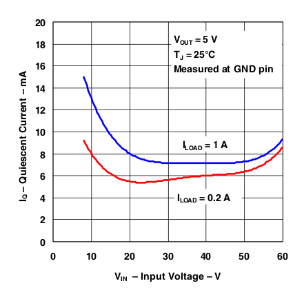 Figure 5. Quiescent Current
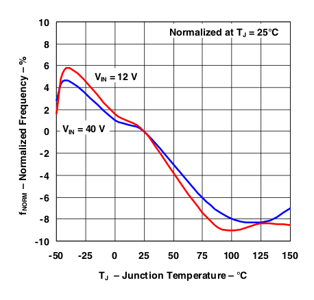 Figure 7. Oscillator Frequency
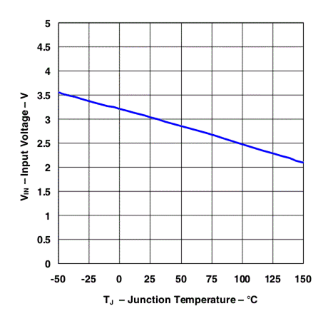 Figure 9. Minimum Operating Voltage
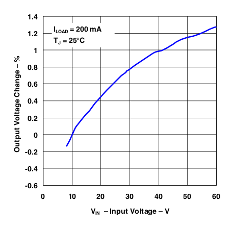 Figure 2. Line Regulation
 Figure 4. Current Limit
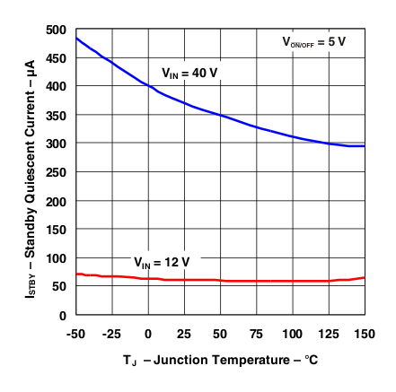 Figure 6. Standby Quiescent Current
 Figure 8. Switch Saturation Voltage
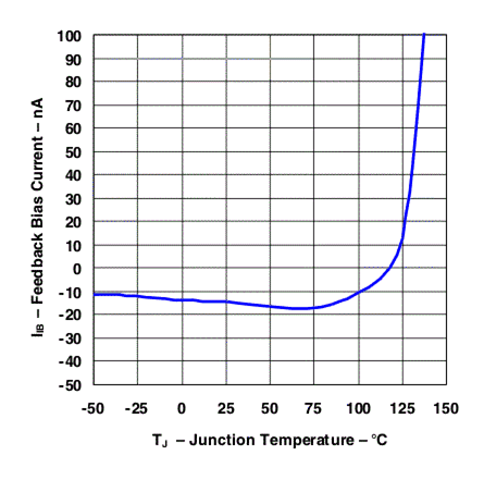 Figure 10. FEEDBACK Current