ZHCS519G April 2000 – May 2019 LM2585
PRODUCTION DATA.
- 1 特性
- 2 应用
- 3 说明
- 4 修订历史记录
- 5 Pin Configurations
-
6 Specifications
- 6.1 Absolute Maximum Ratings
- 6.2 ESD Ratings
- 6.3 Recommended Operating Ratings
- 6.4 Thermal Information
- 6.5 Electrical Characteristics: 3.3 V
- 6.6 Electrical Characteristics: 5 V
- 6.7 Electrical Characteristics: 12-V
- 6.8 Electrical Characteristics: Adjustable
- 6.9 Electrical Characteristics: All Versions
- 6.10 Typical Characteristics
- 7 Detailed Description
- 8 Application and Implementation
- 9 Layout
- 10器件和文档支持
- 11机械、封装和可订购信息
封装选项
机械数据 (封装 | 引脚)
散热焊盘机械数据 (封装 | 引脚)
- KTT|5
订购信息
7.1 Overview
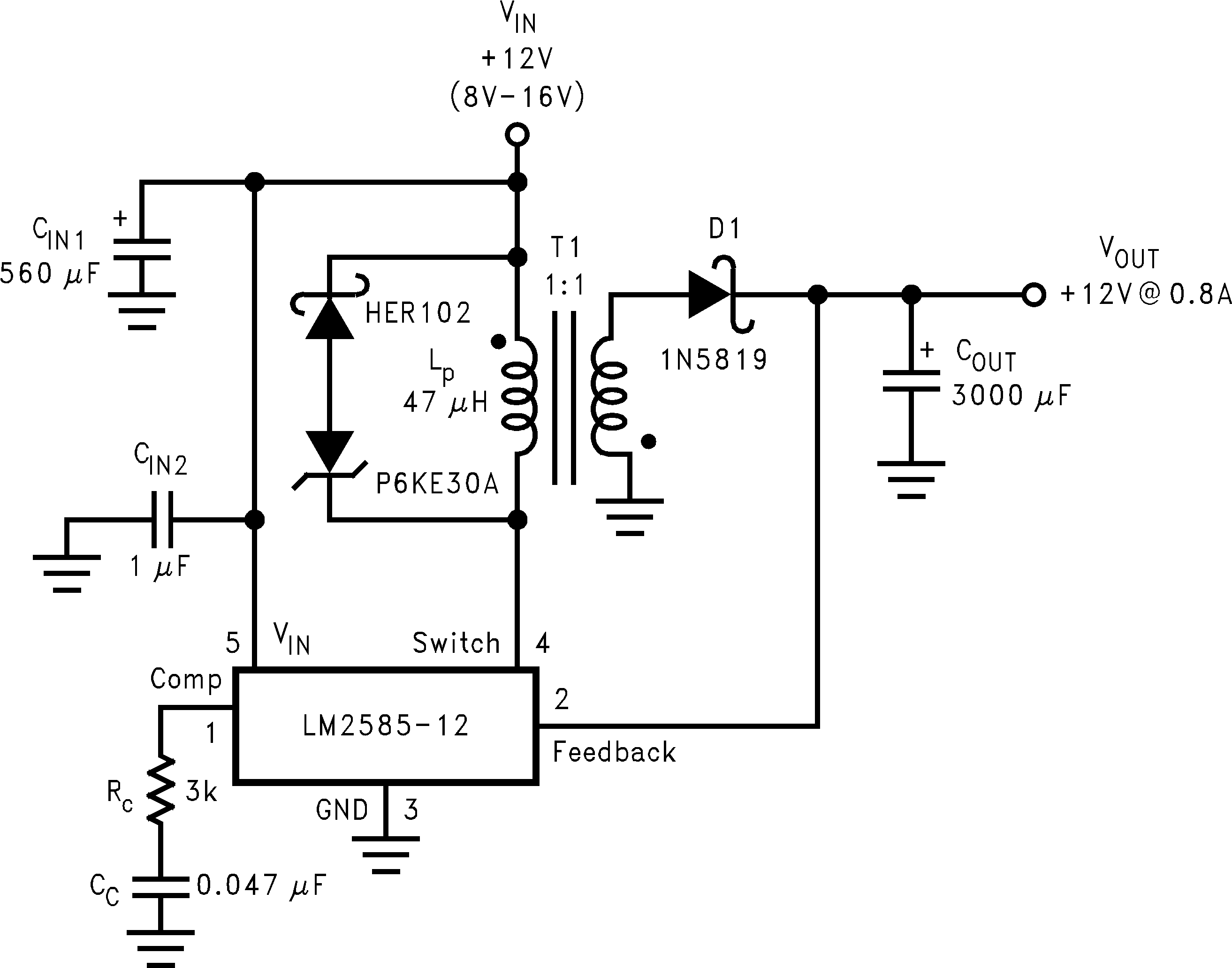
The LM2585 is ideally suited for use in the flyback regulator topology. The flyback regulator can produce a single output voltage, such as the one shown in Figure 12, or multiple output voltages. In Figure 12, the flyback regulator generates an output voltage that is inside the range of the input voltage. This feature is unique to flyback regulators and cannot be duplicated with buck or boost regulators.
The operation of a flyback regulator is as follows (refer to Figure 12): when the switch is on, current flows through the primary winding of the transformer, T1, storing energy in the magnetic field of the transformer. Note that the primary and secondary windings are out of phase, so no current flows through the secondary when current flows through the primary. When the switch turns off, the magnetic field collapses, reversing the voltage polarity of the primary and secondary windings. Now rectifier D1 is forward biased and current flows through it, releasing the energy stored in the transformer. This produces voltage at the output.
The output voltage is controlled by modulating the peak switch current. This is done by feeding back a portion of the output voltage to the error amp, which amplifies the difference between the feedback voltage and a 1.23-V reference. The error amp output voltage is compared to a ramp voltage proportional to the switch current (in other words, inductor current during the switch on time). The comparator terminates the switch on time when the two voltages are equal, thereby controlling the peak switch current to maintain a constant output voltage.
 Figure 12. 12-V Flyback Regulator Design Example
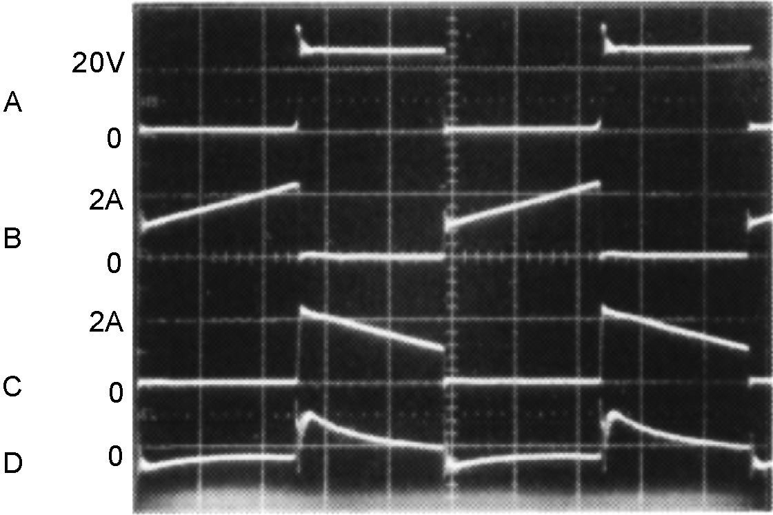
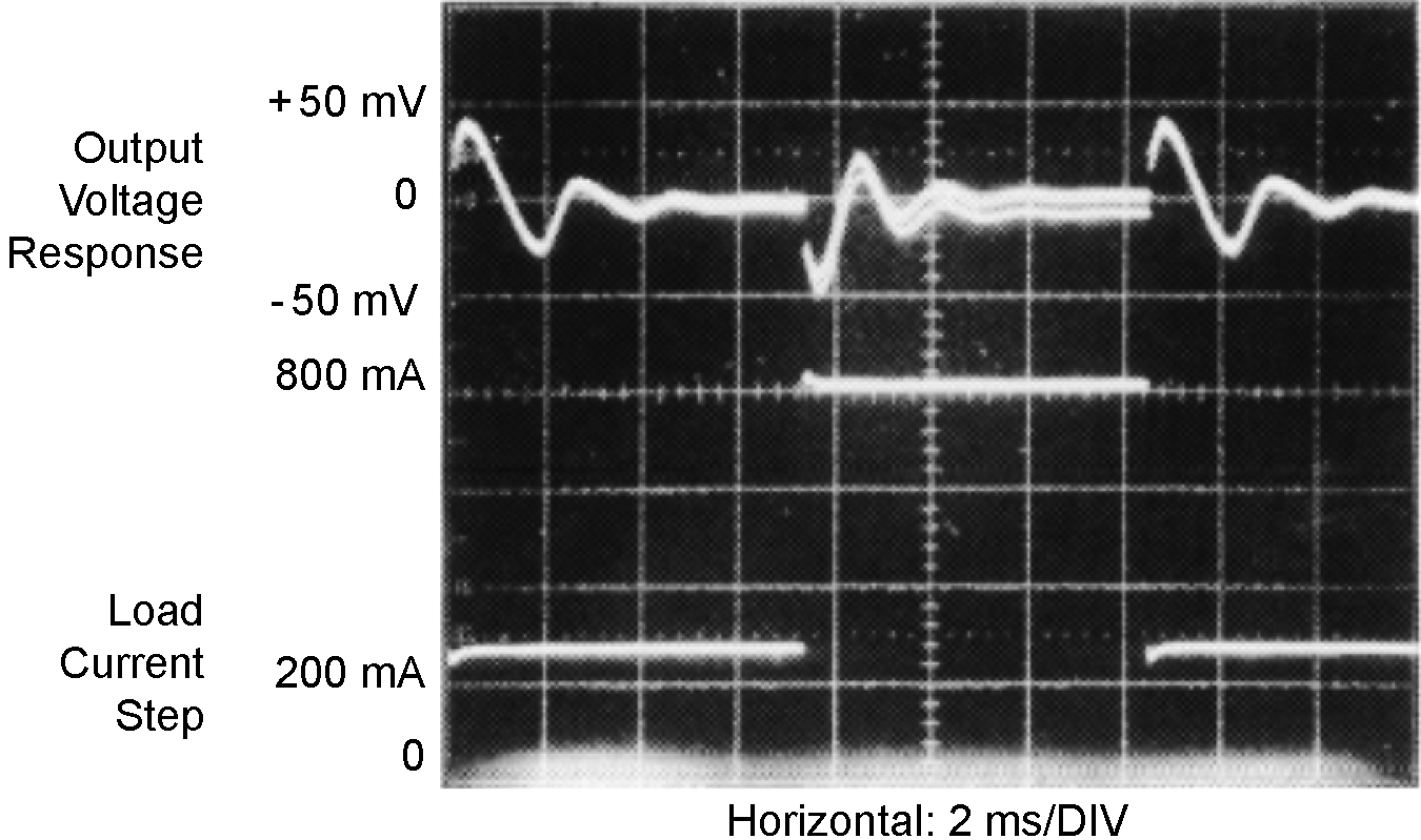
 As shown in Figure 12, the LM2585 can be used as a flyback regulator by using a minimum number of external components. The switching waveforms of this regulator are shown in Figure 13. Typical characteristics observed during the operation of this circuit are shown in Figure 14.

B: Switch Current, 2 A/div
C: Output Rectifier Current, 2 A/div
D: Output Ripple Voltage, 50 mV/div
AC-Coupled
Horizontal: 2 μs/div
 Figure 14. VOUT Load Current Step Response