ZHCS520E May   1996  – May 2019 LM2586

PRODUCTION DATA.  

  1. 特性
  2. 典型 应用
  3. 说明
    1.     Device Images
      1.      方框图
  4. 修订历史记录
  5. Pin Configurations
  6. Specifications
    1. 6.1 Absolute Maximum Ratings
    2. 6.2 ESD Ratings
    3. 6.3 Recommended Operating Ratings
    4. 6.4 Thermal Information
    5. 6.5 Electrical Characteristics: 3.3 V
    6. 6.6 Electrical Characteristics: 5 V
    7. 6.7 Electrical Characteristics: 12 V
    8. 6.8 Electrical Characteristics: Adjustable
    9. 6.9 Typical Characteristics
  7. Detailed Description
    1. 7.1 Overview
    2. 7.2 Functional Block Diagram
    3. 7.3 Feature Description
      1. 7.3.1 Flyback Regulator Operation
      2. 7.3.2 Step-Up (Boost) Regulator Operation
      3. 7.3.3 Programming Output Voltage (Selecting R1 And R2)
      4. 7.3.4 Shutdown Control
      5. 7.3.5 Frequency Adjustment
      6. 7.3.6 Frequency Synchronization
  8. Application and Implementation
    1. 8.1 Application Information
    2. 8.2 Typical Applications
      1. 8.2.1 Typical Flyback Regulator Applications
        1. 8.2.1.1 Design Requirements
          1. 8.2.1.1.1 Transformer Selection (T)
          2. 8.2.1.1.2 Transformer Footprints
        2. 8.2.1.2 Detailed Design Procedure
          1. 8.2.1.2.1 Custom Design With WEBENCH® Tools
          2. 8.2.1.2.2 Flyback Regulator Input Capacitors
          3. 8.2.1.2.3 Switch Voltage Limits
          4. 8.2.1.2.4 Output Voltage Limitations
          5. 8.2.1.2.5 Noisy Input Line Condition
          6. 8.2.1.2.6 Stability
      2. 8.2.2 Typical Boost Regulator Applications
        1. 8.2.2.1 Design Requirements
        2. 8.2.2.2 Detailed Design Procedure
    3. 8.3 System Examples
      1. 8.3.1 Test Circuits
  9. Layout
    1. 9.1 Layout Guidelines
    2. 9.2 Layout Example
  10. 10Heat Sink/Thermal Considerations
  11. 11器件和文档支持
    1. 11.1 器件支持
      1. 11.1.1 第三方米6体育平台手机版_好二三四免责声明
      2. 11.1.2 开发支持
        1. 11.1.2.1 使用 WEBENCH® 工具创建定制设计
    2. 11.2 接收文档更新通知
    3. 11.3 社区资源
    4. 11.4 商标
    5. 11.5 静电放电警告
    6. 11.6 Glossary
  12. 12机械、封装和可订购信息

封装选项

机械数据 (封装 | 引脚)
散热焊盘机械数据 (封装 | 引脚)
订购信息

Step-Up (Boost) Regulator Operation

Figure 20 shows the LM2586 used as a step-up (boost) regulator. This is a switching regulator that produces an output voltage greater than the input supply voltage.

A brief explanation of how the LM2586 boost regulator works is as follows (refer to Figure 20). When the NPN switch turns on, the inductor current ramps up at the rate of VIN/L, storing energy in the inductor. When the switch turns off, the lower end of the inductor flies above VIN, discharging its current through diode (D) into the output capacitor (COUT) at a rate of (VOUT − VIN)/L. Thus, energy stored in the inductor during the switch on time is transferred to the output during the switch off time. The output voltage is controlled by adjusting the peak switch current, as described in .
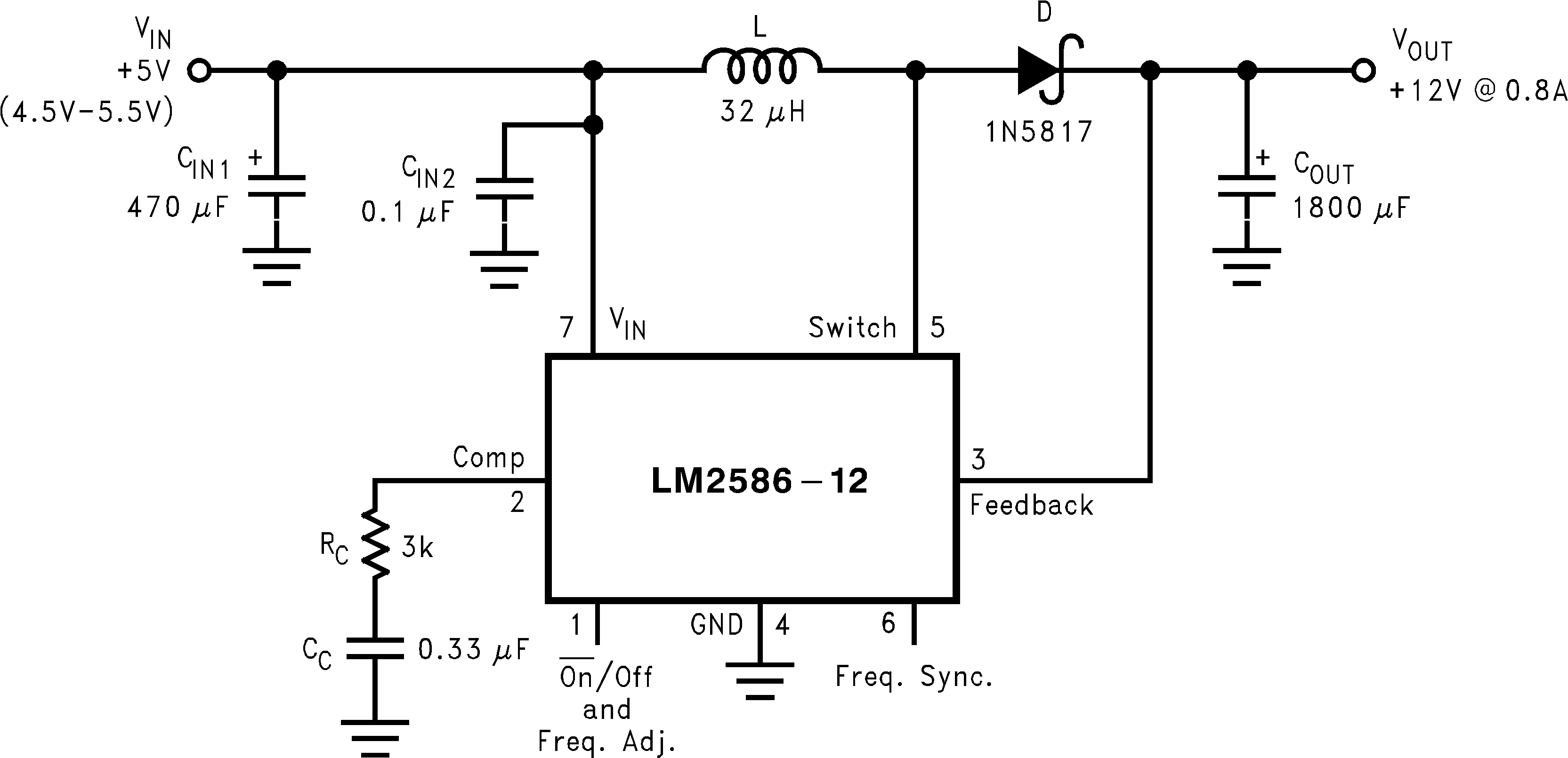
LM2586 01251651.pngFigure 20. 12-V Boost Regulator

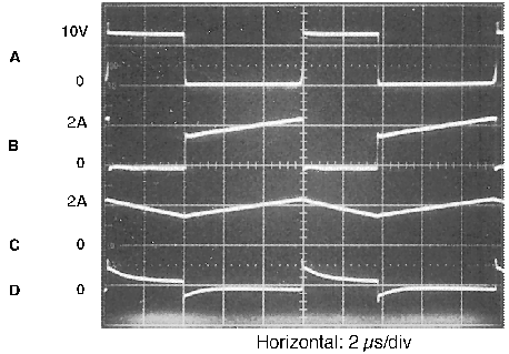
By adding a small number of external components (as shown in Figure 20), the LM2586 can be used to produce a regulated output voltage that is greater than the applied input voltage. The switching waveforms observed during the operation of this circuit are shown in Figure 21. Typical performance of this regulator is shown in Figure 22.
LM2586 01251667.png
A: Switch Voltage,10V/div

B: Switch Current, 2A/div

C: Inductor Current, 2A/div

D: Output Ripple Voltage,100 mV/div, AC-Coupled
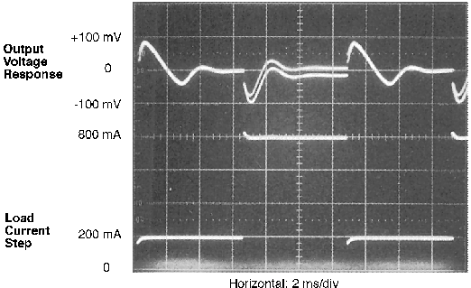
Figure 21. Switching Waveforms
LM2586 01251668.png
Figure 22. VOUT Response To Load Current Step