ZHCS520E May 1996 – May 2019 LM2586
PRODUCTION DATA.
- 1 特性
- 2 典型 应用
- 3 说明
- 4 修订历史记录
- 5 Pin Configurations
- 6 Specifications
- 7 Detailed Description
- 8 Application and Implementation
- 9 Layout
- 10Heat Sink/Thermal Considerations
- 11器件和文档支持
- 12机械、封装和可订购信息
封装选项
机械数据 (封装 | 引脚)
散热焊盘机械数据 (封装 | 引脚)
- KTW|7
订购信息
10 Heat Sink/Thermal Considerations
In many cases, a heat sink is not required to keep the LM2586 junction temperature within the allowed operating temperature range. For each application, to determine whether or not a heat sink will be required, the following must be identified:
1) Maximum ambient temperature (in the application).
2) Maximum regulator power dissipation (in the application).
3) Maximum allowed junction temperature (125°C for the LM2586). For a safe, conservative design, a temperature approximately 15°C cooler than the maximum junction temperature should be selected (110°C).
4) LM2586 package thermal resistances θJA and θJC (given in the Electrical Characteristics).
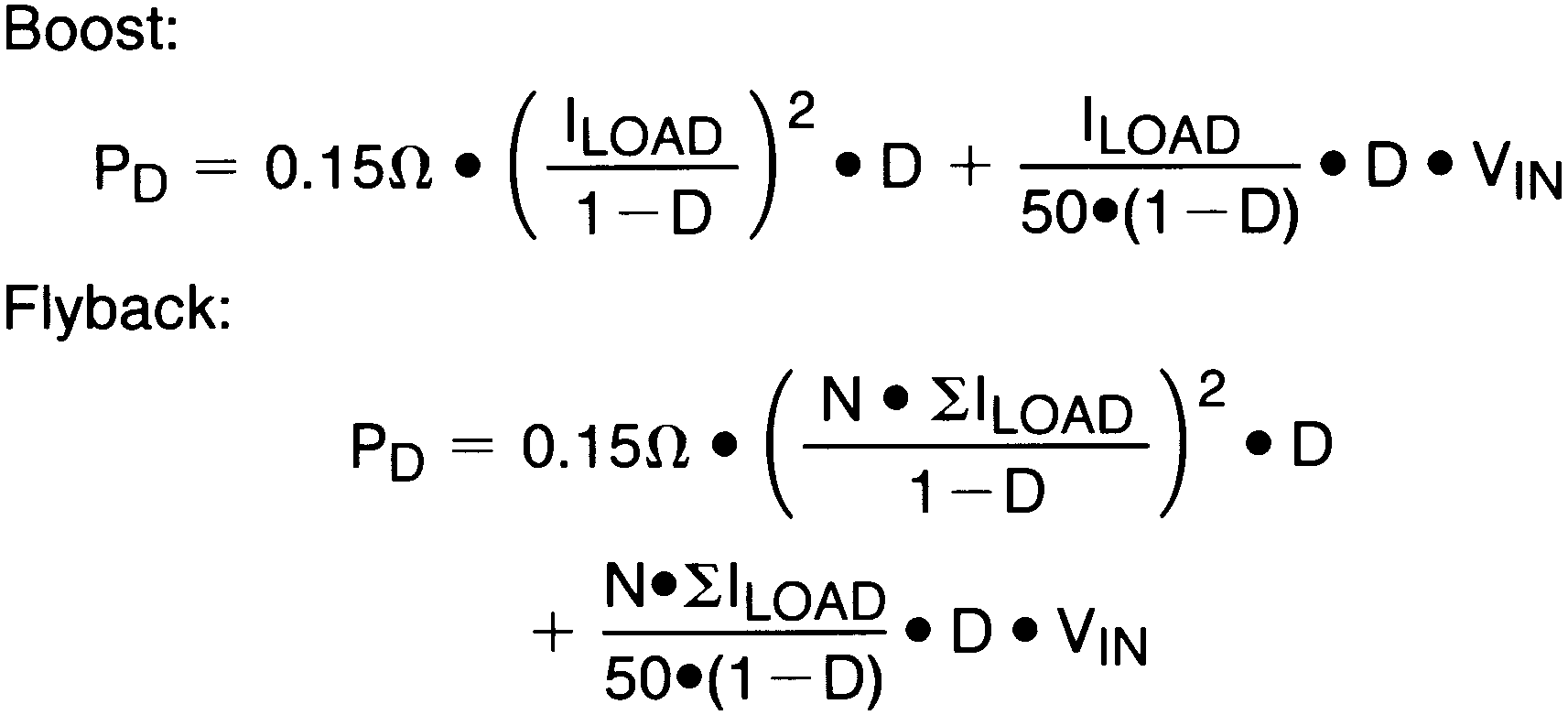
Total power dissipated (PD) by the LM2586 can be estimated as follows:

where
- VIN is the minimum input voltage
- VOUT is the output voltage
- N is the transformer turns ratio, D is the duty cycle
- ILOAD is the maximum load current (and ∑ILOAD is the sum of the maximum load currents for multiple-output flyback regulators)
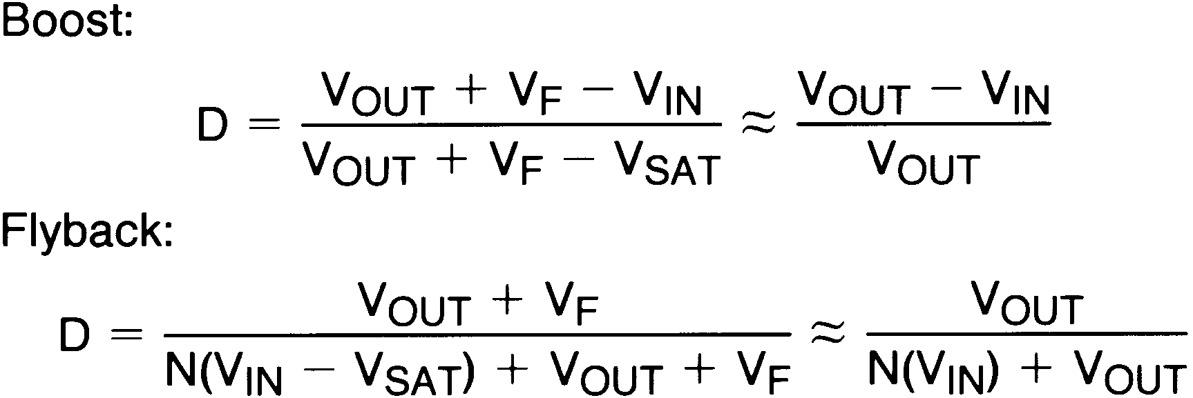
The duty cycle is given by:

where
- VF is the forward biased voltage of the diode and is typically 0.5 V for Schottky diodes and 0.8 V for fast recovery diodes
- VSAT is the switch saturation voltage and can be found in the Characteristic Curves
When no heat sink is used, the junction temperature rise is:
Adding the junction temperature rise to the maximum ambient temperature gives the actual operating junction temperature:
If the operating junction temperature exceeds the maximum junction temperature in item 3 above, then a heat sink is required. When using a heat sink, the junction temperature rise can be determined by the following:
Again, the operating junction temperature will be:
As before, if the maximum junction temperature is exceeded, a larger heat sink is required (one that has a lower thermal resistance).
Included in the Switchers Made Simple® design software is a more precise (non-linear) thermal model that can be used to determine junction temperature with different input-output parameters or different component values. It can also calculate the heat sink thermal resistance required to maintain the regulator junction temperature below the maximum operating temperature.
To further simplify the flyback regulator design procedure, Texas Instruments is making available computer design software to be used with the Simple Switcher ® line of switching regulators.Switchers Made Simple is available on a 3½″ diskette for IBM compatible computers from a Texas Instruments sales office in your area or the Texas Instruments Customer Response Center ((800) 477-8924).