SNVS074E May 2001 – May 2016 LM2591HV
PRODUCTION DATA.
- 1 Features
- 2 Applications
- 3 Description
- 4 Revision History
- 5 Description (continued)
- 6 Pin Configuration and Functions
-
7 Specifications
- 7.1 Absolute Maximum Ratings
- 7.2 ESD Ratings
- 7.3 Recommended Operating Conditions
- 7.4 Thermal Information
- 7.5 Electrical Characteristics LM2591HV-3.3
- 7.6 Electrical Characteristics LM2591HV-5.0
- 7.7 Electrical Characteristics LM2591HV-ADJ
- 7.8 Electrical Characteristics All Output Voltage Versions
- 7.9 Typical Characteristics
- 8 Parameter Measurement Information
- 9 Detailed Description
- 10Application and Implementation
- 11Power Supply Recommendations
- 12Layout
- 13Device and Documentation Support
- 14Mechanical, Packaging, and Orderable Information
封装选项
机械数据 (封装 | 引脚)
散热焊盘机械数据 (封装 | 引脚)
- KTT|5
订购信息
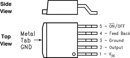
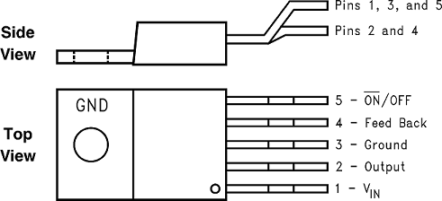
6 Pin Configuration and Functions
KTT Package
5-Pin DDPAK/TO-26
Top View

NDH Package
5-Pin TO-220
Top View

Pin Functions
| PIN | I/O | DESCRIPTION | |
|---|---|---|---|
| NO. | NAME | ||
| 1 | +VIN | I | This is the positive input supply for the IC switching regulator. A suitable input bypass capacitor must be present at this pin to minimize voltage transients and to supply the switching currents needed by the regulator. |
| 2 | Output | O | Internal switch. The voltage at this pin switches between approximately (+VIN − VSAT) and approximately −0.5 V, with a duty cycle of VOUT/VIN. |
| 3 | Ground | — | Circuit ground. |
| 4 | Feedback | I | Senses the regulated output voltage to complete the feedback loop. This pin is directly connected to the Output for the fixed voltage versions, but is set to 1.23 V by means of a resistive divider from the output for the Adjustable version. If a feedforward capacitor is used (Adjustable version), then a negative voltage spike is generated on this pin whenever the output is shorted. This happens because the feedforward capacitor cannot discharge fast enough, and because one end of it is dragged to Ground, the other end goes momentarily negative. To prevent the energy rating of this pin from being exceeded, a small-signal Schottky diode to Ground is recommended for DC input voltages above 40 V whenever a feedforward capacitor is present (See Test Circuits). Feedforward capacitor values larger than 0.1 μF are not recommended for the same reason, whatever be the DC input voltage. |
| 5 | ON/OFF | I | The regulator is in shutdown mode, drawing about 90 μA, when this pin is driven to a high level (≥ 2 V), and is in normal operation when this Pin is left floating or driven to a low level (≤ 0.6 V). The typical value of the threshold is 1.3 V and the voltage on this pin must not exceed 25 V. |