SNVS082E December 2001 – May 2016 LM2593HV
PRODUCTION DATA.
- 1 Features
- 2 Applications
- 3 Description
- 4 Revision History
- 5 Pin Configuration and Functions
-
6 Specifications
- 6.1 Absolute Maximum Ratings
- 6.2 ESD Ratings
- 6.3 Recommended Operating Conditions
- 6.4 Thermal Information
- 6.5 Electrical Characteristics
- 6.6 Electrical Characteristics - 3.3-V Version
- 6.7 Electrical Characteristics - 5-V Version
- 6.8 Electrical Characteristics - Adjustable Voltage Version
- 6.9 Typical Characteristics
- 7 Parameter Measurement Information
- 8 Detailed Description
- 9 Application and Implementation
- 10Power Supply Recommendations
- 11Layout
- 12Device and Documentation Support
- 13Mechanical, Packaging, and Orderable Information
封装选项
机械数据 (封装 | 引脚)
散热焊盘机械数据 (封装 | 引脚)
- KTW|7
订购信息
9 Application and Implementation
NOTE
Information in the following applications sections is not part of the TI component specification, and TI does not warrant its accuracy or completeness. TI’s customers are responsible for determining suitability of components for their purposes. Customers should validate and test their design implementation to confirm system functionality.
9.1 Application Information
9.1.1 Feedforward Capacitor, CFF
(Adjustable output voltage version only)
A feedforward capacitor shown across R2 in Test Circuits is used when the output voltage is greater than 10 V or when COUT has a very low ESR. This capacitor adds lead compensation to the feedback loop and increases the phase margin for better loop stability. If the output voltage ripple is large (>5% of the nominal output voltage), this ripple can be coupled to the feedback pin through the feedforward capacitor and cause the error comparator to trigger the error flag. In this situation, adding a resistor, RFF, in series with the feedforward capacitor, approximately 3 times R1, attenuates the ripple voltage at the feedback pin.
9.1.2 Input Capacitor, CIN
A low-ESR aluminum or tantalum bypass capacitor is needed between the input pin and ground pin. It must be placed near the regulator using short leads. This capacitor prevents large voltage transients from appearing at the input, and provides the instantaneous current needed each time the switch turns on. The important parameters for the Input capacitor are the voltage rating and the RMS current rating. Because of the relatively high RMS currents flowing in a buck regulator’s input capacitor, this capacitor must be chosen for its RMS current rating rather than its capacitance or voltage ratings, although the capacitance value and voltage rating are directly related to the RMS current rating. The voltage rating of the capacitor and its RMS ripple current capability must never be exceeded.
9.1.3 Output Capacitor, COUT
An output capacitor is required to filter the output and provide regulator loop stability. Low impedance or low ESR Electrolytic or solid tantalum capacitors designed for switching regulator applications must be used. When selecting an output capacitor, the important capacitor parameters are; the 100-kHz Equivalent Series Resistance (ESR), the RMS ripple current rating, voltage rating, and capacitance value. For the output capacitor, the ESR value is the most important parameter. The ESR must generally not be less than 100 mW or there will be loop instability. If the ESR is too large, efficiency and output voltage ripple are effected. So ESR must be chosen carefully.
9.1.4 Catch Diode
Buck regulators require a diode to provide a return path for the inductor current when the switch turns off. This must be a fast diode and must be placed close to the LM2593HV using short leads and short printed-circuit traces.
Because of their very fast switching speed and low forward voltage drop, Schottky diodes provide the best performance, especially in low output voltage applications (5 V and lower). Ultra-fast recovery, or high-efficiency rectifiers are also a good choice, but some types with an abrupt turnoff characteristic may cause instability or EMI problems. Ultra-fast recovery diodes typically have reverse recovery times of 50 ns or less. The diode must be chosen for its average or RMS current rating and maximum voltage rating. The voltage rating of the diode must be greater than the DC input voltage (not the output voltage).
9.1.5 lnverting Regulator
The circuit in Figure 31 converts a positive input voltage to a negative output voltage with a common ground. The circuit operates by bootstrapping the regulator’s ground pin to the negative output voltage, then grounding the feedback pin, the regulator senses the inverted output voltage and regulates it. This example uses the LM2593HV 5-V to generate a −5-V output, but other output voltages are possible by selecting other output voltage versions, including the adjustable version. Because this regulator topology can produce an output voltage that is either greater than or less than the input voltage, the maximum output current greatly depends on both the input and output voltage. To determine how much load current is possible before the internal device current limit is reached (and power limiting occurs), the system must be evaluated as a buck-boost configuration rather than as a buck. The peak switch current in amperes, for such a configuration is given as Equation 1.

where
- L is in μH
- f is in Hz
The maximum possible load current ILOAD is limited by the requirement that IPEAK ≤ ICLIM. While checking for this, take ICLIM to be the lowest possible current limit value (minimum across tolerance and temperature is 2.3 A for the LM2593HV). Also to account for inductor tolerances, take the minimum value of Inductance for L in Equation 1 (typically 20% less than the nominal value). Further, the above equation disregards the drop across the switch and the diode. This is equivalent to assuming 100% efficiency, which is never so. Therefore expect IPEAK to be an additional 10-20% higher than calculated from Equation 1. See also Application Note AN-1197 Selecting Inductors for Buck Converters (SNVA038) for examples based on positive to negative configuration. The maximum voltage appearing across the regulator is the absolute sum of the input and output voltage. This must be limited to a maximum of 60 V. In this example, when converting 20 V to −5 V, the regulator would see 25 V between the input pin and ground pin. The LM2593HV has a maximum input voltage rating of 60 V. An additional diode is required in this regulator configuration. Diode D1 is used to isolate input voltage ripple or noise from coupling through the CIN capacitor to the output, under light or no load conditions. Also, this diode isolation changes the topology to closely resemble a buck configuration thus providing good closed-loop stability. A Schottky diode is recommended for low input voltages, (because of its lower voltage drop) but for higher input voltages, a IN5400 diode could be used. Because of differences in the operation of the inverting regulator, the standard design procedure is not used to select the inductor value. In the majority of designs, a 33-μH, 4-A inductor is the best choice. Capacitor selection can also be narrowed down to just a few values. This type of inverting regulator can require relatively large amounts of input current when starting up, even with light loads. Input currents as high as the LM2593HV current limit (approximately 4 A) are needed for 2 ms or more, until the output reaches its nominal output voltage. The actual time depends on the output voltage and the size of the output capacitor. Input power sources that are current limited or sources that can not deliver these currents without getting loaded down, may not work correctly. Because of the relatively high start-up currents required by the inverting topology, the soft-start feature shown in Figure 31 is recommended. Also shown in Figure 31 are several shutdown methods for the inverting configuration. With the inverting configuration, some level shifting is required, because the ground pin of the regulator is no longer at ground, but is now at the negative output voltage. The shutdown methods shown accept ground referenced shutdown signals.
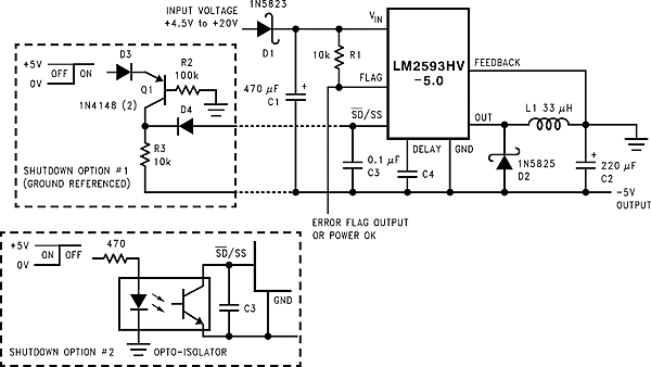 Figure 31. Inverting −5 V Regulator With Shutdown and Soft-Start
9.2 Typical Application
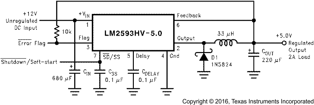 Figure 32. LM2593HV 5-V Application Schematic
9.2.1 Design Requirements
Table 1 lists the example values for this typical application.
Table 1. Application Example Parameters
| DESIGN PARAMETER | EXAMPLE VALUE |
|---|---|
| Regulated output voltage (3.3 V, 5 V, or adjustable), VOUT | 5 V |
| Maximum input voltage, VIN(max) | 24 V |
| Maximum load current, ILOAD(max) | 1 A |
| Switching frequency, F | Fixed at a nominal 150 kHz |
9.2.2 Detailed Design Procedure
9.2.2.1 Inductors Selection Procedure
See application note AN-1197 Selecting Inductors for Buck Converters (SNVA038) for detailed information on inductor selection. For a quick-start, see the nomographs provided in Figure 33 to Figure 35. To widen the choices to a more general selection of available inductors, the nomographs provide the required inductance and also the energy in the core expressed in microjoules (μJ), as an alternative to just prescribing custom parts. The following points must be highlighted:
- The energy values shown on the nomographs apply to steady operation at the corresponding x-coordinate (rated maximum load current). However under start-up, without soft-start, or a short-circuit on the output, the current in the inductor momentarily and repetitively hits the current limit ICLIM of the device, and this current could be much higher than the rated load, ILOAD. This represents an overload situation, and can cause the inductor to saturate (if it has been designed only to handle the energy of steady operation). However most types of core structures used for such applications have a large inherent air gap (for example powdered iron types or ferrite rod inductors), and so the inductance does not fall off too sharply under an overload. The device is usually able to protect itself by not allowing the current to ever exceed ICLIM. But if the DC input voltage to the regulator is over 40 V, the current can slew up so fast under core saturation, that the device may not be able to act fast enough to restrict the current. The current can then rise without limit till destruction of the device takes place. Therefore to ensure reliability, TI recommends, that if the DC input voltage exceeds 40 V, the inductor must always be sized to handle an instantaneous current equal to ICLIM without saturating, irrespective of the type of core structure or material.
- Use Equation 2 to calculate the energy under steady operation.
- L is in μH
- IPEAK is the peak of the inductor current waveform with the regulator delivering ILOAD
- The energy under overload is Equation 3.
- L is in μH
- IPEAK is the peak of the inductor current waveform with the regulator delivering ILOAD
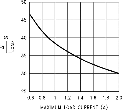
- The nomographs were generated by allowing a greater amount of percentage current ripple in the inductor as the maximum rated load decreases (see Figure 36). This was done to permit the use of smaller inductors at light loads. However, Figure 36 shows only the median value of the current ripple. In reality there may be a great spread around this because the nomographs approximate the exact calculated inductance to standard available values. It is a good idea to refer to AN-1197 Selecting Inductors for Buck Converters (SNVA038) for detailed calculations if a certain maximum inductor current ripple is required for various possible reasons. Also consider the rather wide tolerance on the nominal inductance of commercial inductors.
- Figure 35 shows the inductor selection curves for the adjustable version. The y-axis is Et, in Vμs. It is the applied volts across the inductor during the ON time of the switch (VIN-VSAT-VOUT) multiplied by the time for which the switch is on in μs. See Example 3.

where
These are the energy values shown in the nomographs. See Example 1.

where
If VIN > 40 V, the inductor must be sized to handle eCLIM instead of the steady energy values. The worst case ICLIM for the LM2593HV is 4 A. The energy rating depends on the inductance. See Example 2.
9.2.2.1.1 Example 1: VIN ≤ 40 V, 5-V Version, VIN = 24 V, Output = 5 V at 1 A
- A first pass inductor selection is based upon inductance and rated maximum load current. Choose an inductor with the inductance value indicated by the nomograph (see Figure 34) and a current rating equal to the maximum load current. Therefore, quick-select a 68-μH, 1-A inductor (designed for 150-kHz operation) for this application.
- Confirm that it is rated to handle 50 μJ (see Figure 34) by either estimating the peak current or by a detailed calculation as shown in AN-1197 Selecting Inductors for Buck Converters (SNVA038), and also that the losses are acceptable.
9.2.2.1.2 Example 2: VIN > 40 V, 5-V version, VIN = 48 V, Output = 5 V at 1.5 A
- A first pass inductor selection is based upon inductance and the switch currrent limit. Choose an inductor with the inductance value indicated by the nomograph (see Figure 34) and a current rating equal to ICLIM. Therefore, quick-select a 68-μH, 4-A inductor (designed for 150-kHz operation) for this application.
- Confirm that it is rated to handle eCLIM by the procedure shown in AN-1197 Selecting Inductors for Buck Converters (SNVA038) and that the losses are acceptable. Here eCLIM is Equation 4.

9.2.2.1.3 Example 3: VIN ≤ 40 V, Adjustable Version, VIN = 20 V, Output = 10 V at 2 A
- Because input voltage is less than 40 V, a first pass inductor selection is based upon inductance and rated maximum load current. Choose an inductor with the inductance value indicated by the nomograph Figure 35 and a current rating equal to the maximum load. But first calculate Et for the given application. The duty cycle is Equation 5.
- VD is the drop across the catch diode (0.5 V for a Schottky)
- VSAT the drop across the switch (1.5 V)
- The switch ON time is calculated with Equation 7.
- f is the switching frequency in Hz
- Therefore, looking at Figure 33, quick-select a 47-μH, 2-A inductor (designed for 150-kHz operation) for this application.
- Confirm that it is rated to handle 200 μJ (see Figure 35) by the procedure shown in AN-1197 Selecting Inductors for Buck Converters (SNVA038) and that the losses are acceptable. (If the DC input voltage had been greater than 40 V, consider eCLIM as in Example 2).

where
So this yields Equation 6.


where
So this yields Equation 8.

This completes the simplified inductor selection procedure. For more general applications and better optimization, refer to AN-1197 Selecting Inductors for Buck Converters (SNVA038).
9.2.3 Application Curves
For continuous mode operation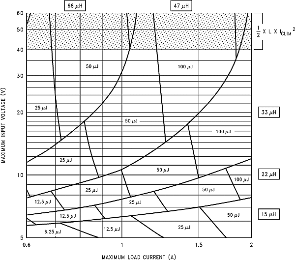 Figure 33. LM2593HV 3.3-V
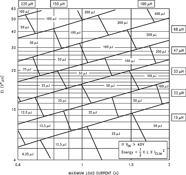 Figure 35. LM2593HV Adjustable Voltage
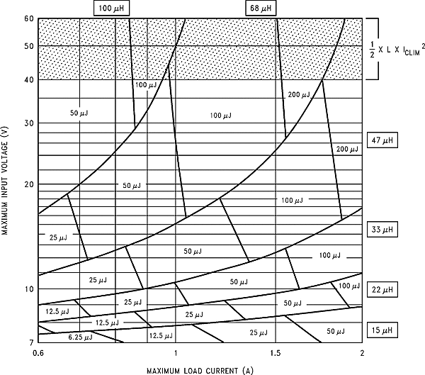 Figure 34. LM2593HV 5-V
