SNVS082E December 2001 – May 2016 LM2593HV
PRODUCTION DATA.
- 1 Features
- 2 Applications
- 3 Description
- 4 Revision History
- 5 Pin Configuration and Functions
-
6 Specifications
- 6.1 Absolute Maximum Ratings
- 6.2 ESD Ratings
- 6.3 Recommended Operating Conditions
- 6.4 Thermal Information
- 6.5 Electrical Characteristics
- 6.6 Electrical Characteristics - 3.3-V Version
- 6.7 Electrical Characteristics - 5-V Version
- 6.8 Electrical Characteristics - Adjustable Voltage Version
- 6.9 Typical Characteristics
- 7 Parameter Measurement Information
- 8 Detailed Description
- 9 Application and Implementation
- 10Power Supply Recommendations
- 11Layout
- 12Device and Documentation Support
- 13Mechanical, Packaging, and Orderable Information
封装选项
机械数据 (封装 | 引脚)
散热焊盘机械数据 (封装 | 引脚)
- KTW|7
订购信息
11 Layout
11.1 Layout Guidelines
As in any switching regulator, layout is very important. Rapid switching currents associated with wiring inductance can generate voltage transients which can cause problems. For minimal inductance and ground loops, with reference to Functional Block Diagram, the wires indicated by heavy lines must be wide printed-circuit traces and must be kept as short as possible. For best results, external components must be placed as close to the switcher lC as possible using ground plane construction or single-point grounding.
If open core inductors are used, take special care as to the location and positioning of this type of inductor. Allowing the inductor flux to intersect sensitive feedback, lC groundpath and COUT wiring can cause problems.
When using the adjustable version, take special care as to the location of the feedback resistors and the associated wiring. Physically place both resistors near the IC, and route the wiring away from the inductor, especially an open core type of inductor.
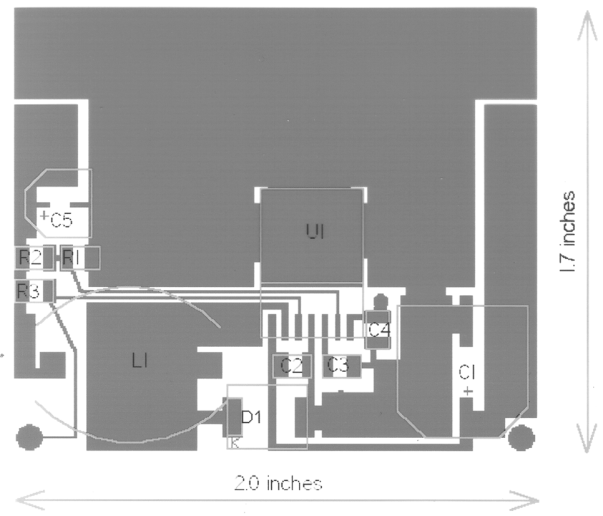
11.2 Layout Example
 Figure 37. Top Side (Component Side) of PCB
11.3 Thermal Considerations
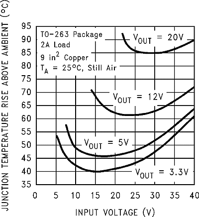
The LM2593HV is available in two packages, a 5-pin TO-220 (T) and a 5-pin surface-mount TO-263 (S). The TO-220 package needs a heat sink under most conditions. The size of the heat sink depends on the input voltage, the output voltage, the load current, and the ambient temperature. Higher ambient temperatures require more heat sinking. The TO-263 surface-mount package tab is designed to be soldered to the copper on a printed-circuit board. The copper and the board are the heat sink for this package and the other heat-producing components, such as the catch diode and inductor. The PCB copper area that the package is soldered to must be at least 0.4 in2, and ideally must have 2 or more square inches of 2-oz. (0.0028 in) copper. Additional copper area improves the thermal characteristics, but with copper areas greater than approximately 6 in2, only small improvements in heat dissipation are realized. If further thermal improvements are needed, double-sided, multilayer PCB with large copper areas or airflow are recommended. The curves shown in Figure 38 show the LM2593HVS (TO-263 package) junction temperature rise above ambient temperature with a 2-A load for various input and output voltages. This data was taken with the circuit operating as a buck switching regulator with all components mounted on a PCB to simulate the junction temperature under actual operating conditions. This curve can be used for a quick check for the approximate junction temperature for various conditions, but be aware that there are many factors that can affect the junction temperature. When load currents higher than 2 A are used, double-sided or multilayer PCBs with large copper areas or airflow might be required, especially for high ambient temperatures and high output voltages. For the best thermal performance, wide copper traces and generous amounts of printed-circuit board copper must be used in the board layout. (One exception to this is the output (switch) pin, which must not have large areas of copper.) Large areas of copper provide the best transfer of heat (lower thermal resistance) to the surrounding air, and moving air lowers the thermal resistance even further. Package thermal resistance and junction temperature rise numbers are all approximate, and there are many factors that affect these numbers. Some of these factors include board size, shape, thickness, position, location, and even board temperature. Other factors are, trace width, total printed-circuit copper area, copper thickness, single- or double-sided, multilayer board, and the amount of solder on the board. The effectiveness of the PCB to dissipate heat also depends on the size, quantity, and spacing of other components on the board, as well as whether the surrounding air is still or moving. Furthermore, some of these components, such as the catch diode will add heat to the PCB and the heat can vary as the input voltage changes. For the inductor, depending on the physical size, type of core material, and the DC resistance, it could either act as a heat sink taking heat away from the board, or it could add heat to the board.
 Figure 38. Junction Temperature Rise, TO-263