SNVS118F december 1999 – may 2023 LM2594 , LM2594HV
PRODUCTION DATA
- 1
- 1 Features
- 2 Applications
- 3 Description
- 4 Revision History
- 5 Description (continued)
- 6 Pin Configuration and Functions
-
7 Specifications
- 7.1 Absolute Maximum Ratings
- 7.2 ESD Ratings
- 7.3 Recommended Operating Conditions
- 7.4 Thermal Information
- 7.5 Electrical Characteristics – 3.3 V
- 7.6 Electrical Characteristics – 5 V
- 7.7 Electrical Characteristics – 12 V
- 7.8 Electrical Characteristics – Adjustable
- 7.9 Electrical Characteristics – All Output Voltage Versions
- 7.10 Typical Characteristics
- 8 Detailed Description
- 9 Application and Implementation
- 10Device and Documentation Support
- 11Mechanical, Packaging, and Orderable Information
8.3.3 Inverting Regulator
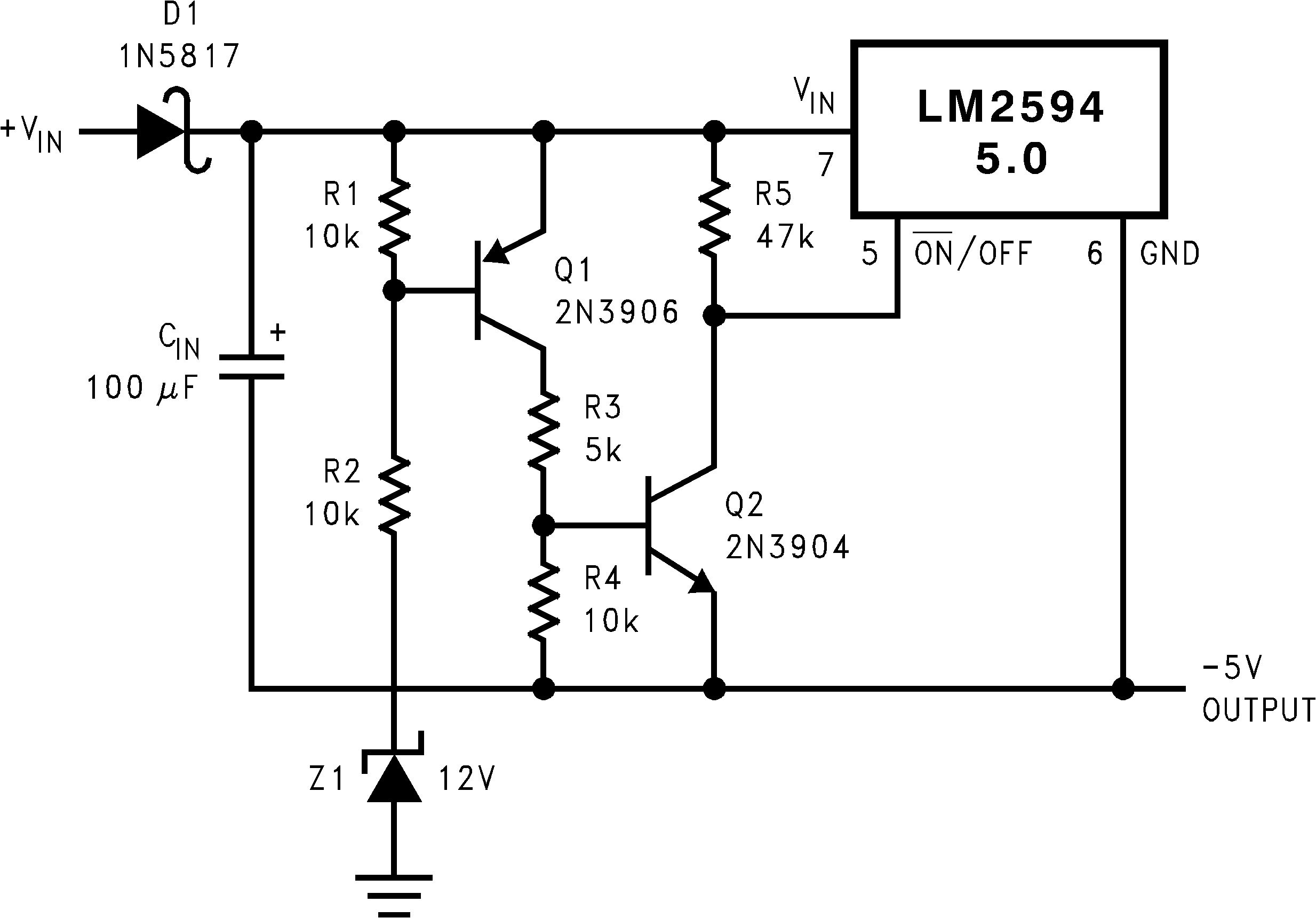
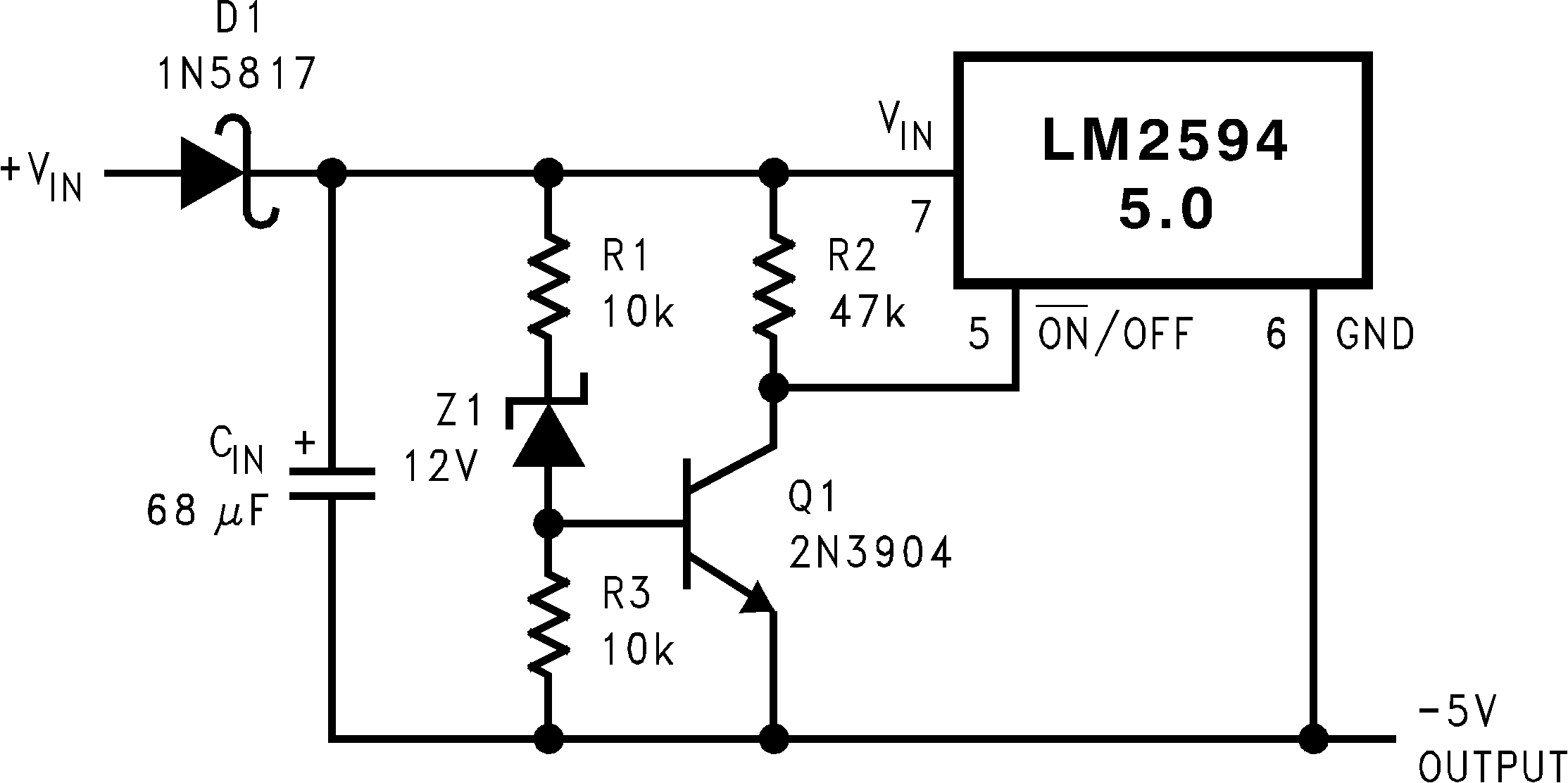
The circuit in Figure 8-5 converts a positive input voltage to a negative output voltage with a common ground. The circuit operates by bootstrapping the regulators ground pin to the negative output voltage, then grounding the feedback pin, the regulator senses the inverted output voltage and regulates it.


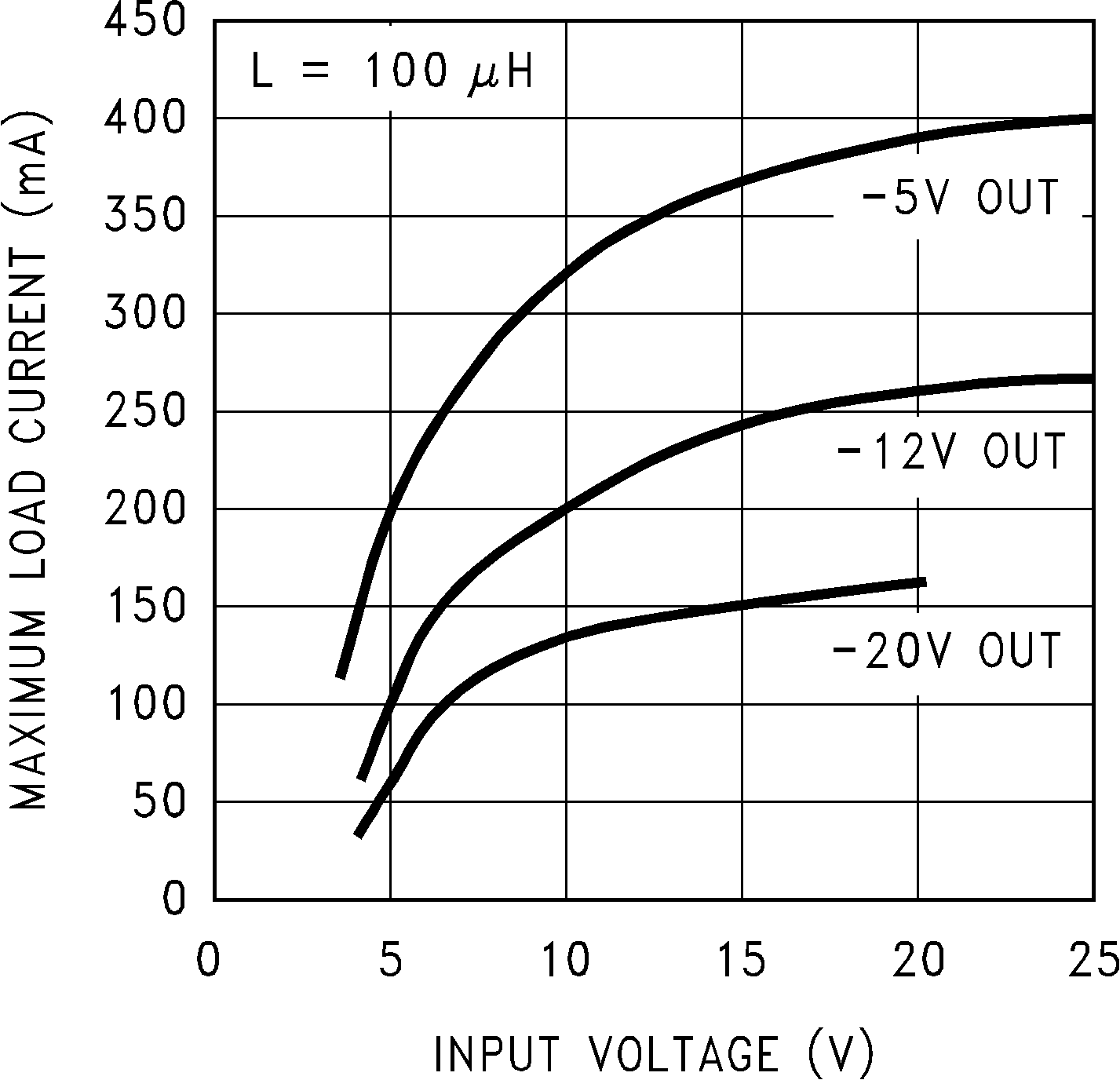
This example uses the LM2594-5 to generate a −5-V output, but other output voltages are possible by selecting other output voltage versions, including the adjustable version. Because this regulator topology can produce an output voltage that is either greater than or less than the input voltage, the maximum output current greatly depends on both the input and output voltage. Figure 8-6 provides a guide as to the amount of output load current possible for the different input and output voltage conditions.
The maximum voltage appearing across the regulator is the absolute sum of the input and output voltage, and this must be limited to a maximum of 40 V. For example, when converting 20 V to −12 V, the regulator can see 32 V between the input pin and ground pin. The LM2594 has a maximum input voltage specification of 40 V (60 V for the LM2594HV).
Additional diodes are required in this regulator configuration. Diode D1 is used to isolate input voltage ripple or noise from coupling through the CIN capacitor to the output, under light or no load conditions. Also, this diode isolation changes the topology to closely resemble a buck configuration thus providing good closed loop stability. TI recommends a Schottky diode for low input voltages (because of its lower voltage drop), but for higher input voltages, a fast recovery diode can be used.
Without diode D3, when the input voltage is first applied, the charging current of CIN can pull the output positive by several volts for a short period of time. Adding D3 prevents the output from going positive by more than a diode voltage.
 Figure 8-6 Inverting Regulator Typical Load Current
Because of differences in the operation of the inverting regulator, the standard design procedure is not used to select the inductor value. In the majority of designs, a 100-μH, 1-A inductor is the best choice. Capacitor selection can also be narrowed down to just a few values. Using the values shown in Figure 8-5 provides good results in the majority of inverting designs.
This type of inverting regulator can require relatively large amounts of input current when starting up, even with light loads. Input currents as high as the LM2594 current limit (approximately 0.8 A) are needed for at least 2 ms or more, until the output reaches its nominal output voltage. The actual time depends on the output voltage and the size of the output capacitor. Input power sources that are current limited or sources that can not deliver these currents without getting loaded down, can not work correctly. Because of the relatively high start-up currents required by the inverting topology, the delayed start-up feature (C1, R1 and R2) shown in Figure 8-5 is recommended. By delaying the regulator start-up, the input capacitor is allowed to charge up to a higher voltage before the switcher begins operating. A portion of the high input current needed for start-up is now supplied by the input capacitor (CIN). For severe start-up conditions, the input capacitor can be made much larger than normal.