SNVS119D March 1998 – May 2016 LM2597 , LM2597HV
PRODUCTION DATA.
- 1 Features
- 2 Applications
- 3 Description
- 4 Revision History
- 5 Description (continued)
- 6 Pin Configuration and Functions
-
7 Specifications
- 7.1 Absolute Maximum Ratings
- 7.2 ESD Ratings
- 7.3 Recommended Operating Conditions
- 7.4 Thermal Information
- 7.5 Electrical Characteristics - 3.3 V
- 7.6 Electrical Characteristics - 5 V
- 7.7 Electrical Characteristics - 12 V
- 7.8 Electrical Characteristics - Adjustable
- 7.9 Electrical Characteristics - All Output Voltage Versions
- 7.10 Typical Characteristics
- 8 Detailed Description
- 9 Application and Implementation
- 10Power Supply Recommendations
- 11Layout
- 12Device and Documentation Support
- 13Mechanical, Packaging, and Orderable Information
11 Layout
11.1 Layout Guidelines
As in any switching regulator, layout is very important. Rapidly switching currents associated with wiring inductance can generate voltage transients which can cause problems. For minimal inductance and ground loops, the wires indicated by heavy lines must be wide printed-circuit traces and must be kept as short as possible. For best results, external components must be placed as close to the switcher lC as possible using ground plane construction or single point grounding.
If open core inductors are used, take care of the location and positioning of this type of inductor. Allowing the inductor flux to intersect sensitive feedback, lC groundpath and COUT wiring can cause problems.
When using the adjustable version, take special care regarding the location of the feedback resistors and the associated wiring. Physically place both resistors near the IC, and route the wiring away from the inductor, especially an open core type of inductor.
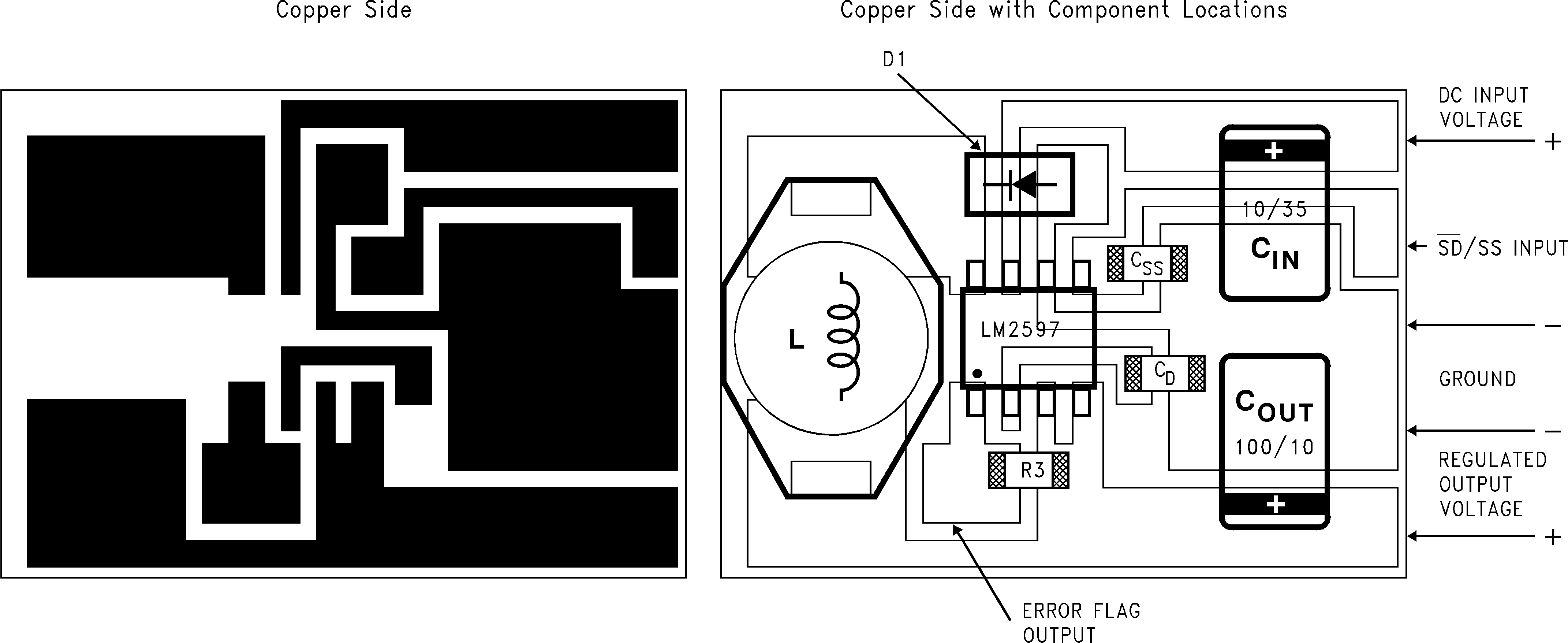
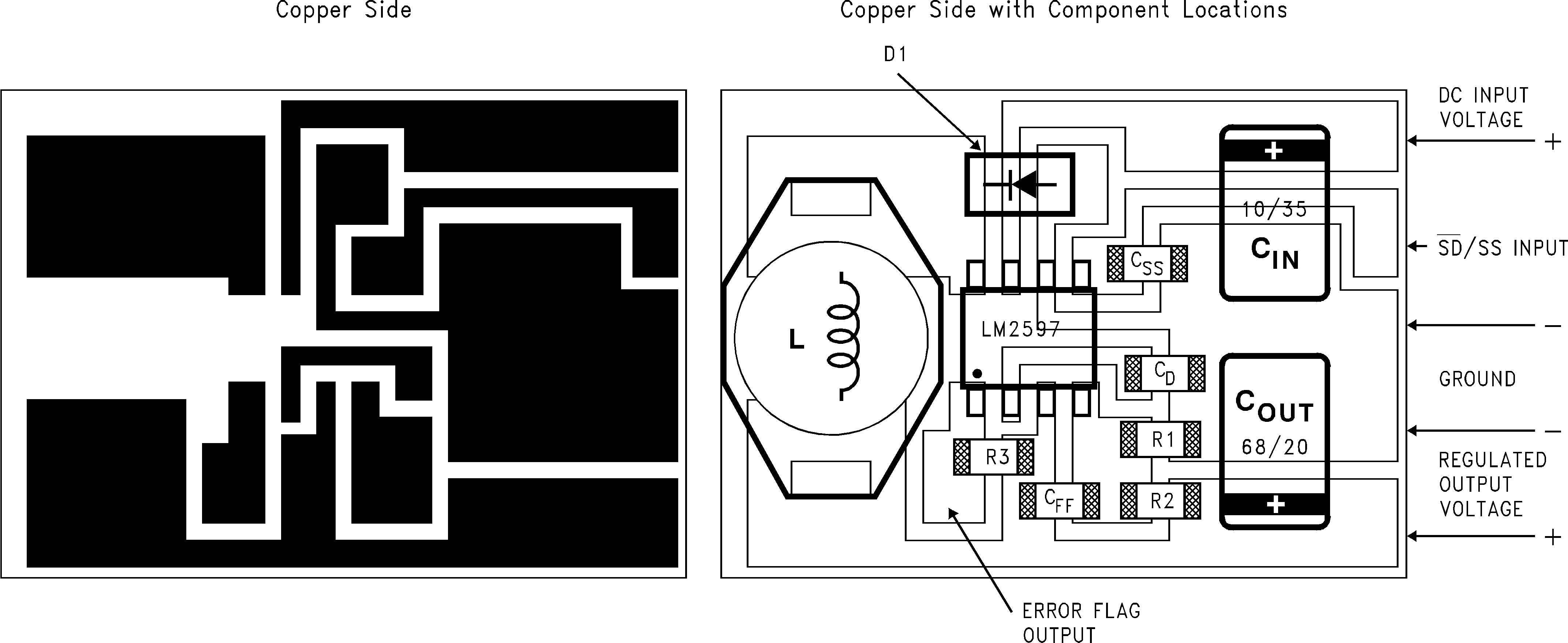
11.2 Layout Example

COUT – 100-µF, 10-V solid tantalum, AVX, TPS Series (surface-mount, D size)
D1 – 1-A, 40-V surface-mount, Schottky rectifier
L1 – Surface-mount inductor, Coilcraft DO33
CSS – Soft-start capacitor (surface-mount, ceramic chip capacitor)
CD – Delay capacitor (surface-mount, ceramic chip capacitor)
R3 – Error flag pullup resistor (surface-mount, chip resistor)

COUT – 68-μF, 20-V solid tantalum, AVX, TPS Series (surface-mount, D size)
D1 – 1-A, 40-V Surface-mount, Schottky rectifier
L1 – Surface-mount inductor, Coilcraft DO33
CSS – Soft-start capacitor (surface-mount, ceramic chip capacitor)
CD – Delay capacitor (surface-mount, ceramic chip capacitor)
CFF – Feedforward capacitor (surface-mount, ceramic chip capacitor)
R1 – Output voltage program resistor (surface-mount, chip resistor)
R2 – Output voltage program resistor (surface-mount, chip resistor)
R3 – Error flag pullup resistor (surface-mount, chip resistor)
11.3 Thermal Considerations
The LM2597xx is available in two packages: an 8-pin through-hole PDIP (P) and an 8-pin surface-mount SOIC (D).Both packages are molded plastic with a copper lead frame. When the package is soldered to the PCB, the copper and the board are the heat sink for the LM2597 and the other heat producing components.
For best thermal performance, wide copper traces must be used. Pins must be soldered to generous amounts of printed-circuit board (PCB) copper, (one exception to this is the output (switch) pin, which must not have large areas of copper). Large areas of copper provide the best transfer of heat (lower thermal resistance) to the surrounding air, and even double-sided or multilayer boards provide a better heat path to the surrounding air. Unless power levels are small, sockets are not recommended because of the added thermal resistance it adds and the resultant higher junction temperatures.
Package thermal resistance and junction temperature rise numbers are all approximate, and there are many factors that will affect the junction temperature. Some of these factors include board size, shape, thickness, position, location, and even board temperature. Other factors are trace width, printed-circuit copper area, copper thickness, single- or double-sided multilayer board, and the amount of solder on the board. The effectiveness of the PCB to dissipate heat also depends on the size, quantity, and spacing of other components on the board. Furthermore, some of these components such as the catch diode will add heat to the PCB and the heat can vary as the input voltage changes. For the inductor, depending on the physical size, type of core material, and the DC resistance, it could either act as a heat sink taking heat away from the board, or it could add heat to the board.

| Circuit Data for Temperature Rise Curve | |
| Capacitors | Through hole electrolytic |
| Inductor | Through hole, Schott, 100 μH |
| Diode | Through hole, 1-A, 40-V, Schottky |
| PCB | 4 square inches single sided 2 oz. copper (0.0028″) |

| Circuit Data for Temperature Rise Curve (Surface Mount) | |
| Capacitors | Through hole electrolytic |
| Inductor | Through hole, Schott, 100 μH |
| Diode | Through hole, 1-A, 40-V, Schottky |
| PCB | 4 square inches single sided 2 oz. copper (0.0028″) |
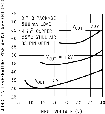
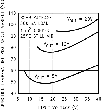
Figure 51 and Figure 52 show the LM2597 junction temperature rise above ambient temperature with a 500-mA load for various input and output voltages. The Bias Supply pin was not used (left open) for these curves. Connecting the Bias Supply pin to the output voltage would reduce the junction temperature by approximately 5°C to 15°C, depending on the input and output voltages, and the load current. This data was taken with the circuit operating as a buck switcher with all components mounted on a PCB to simulate the junction temperature under actual operating conditions. This curve is typical, and can be used for a quick check on the maximum junction temperature for various conditions, but keep in mind that there are many factors that can affect the junction temperature.