SNVS119D March 1998 – May 2016 LM2597 , LM2597HV
PRODUCTION DATA.
- 1 Features
- 2 Applications
- 3 Description
- 4 Revision History
- 5 Description (continued)
- 6 Pin Configuration and Functions
-
7 Specifications
- 7.1 Absolute Maximum Ratings
- 7.2 ESD Ratings
- 7.3 Recommended Operating Conditions
- 7.4 Thermal Information
- 7.5 Electrical Characteristics - 3.3 V
- 7.6 Electrical Characteristics - 5 V
- 7.7 Electrical Characteristics - 12 V
- 7.8 Electrical Characteristics - Adjustable
- 7.9 Electrical Characteristics - All Output Voltage Versions
- 7.10 Typical Characteristics
- 8 Detailed Description
- 9 Application and Implementation
- 10Power Supply Recommendations
- 11Layout
- 12Device and Documentation Support
- 13Mechanical, Packaging, and Orderable Information
8 Detailed Description
8.1 Overview
The LM2597 SIMPLE SWITCHER® regulator is an easy-to-use, nonsynchronous step-down DC-DC converter with a wide input voltage range from 45 V to up to 60 V for the HV version. The regulatorm is capable of delivering up to 0.5-A DC load current with excellent line and load regulation. These devices are available in fixed output voltages of 3.3-V, 5-V, 12-V, and an adjustable output version. The family requires few external components, and the pin arrangement was designed for simple, optimum PCB layout.
8.2 Functional Block Diagram

8.3 Feature Description
8.3.1 Bias Supply Feature
The bias supply (VBS) pin allows the internal circuitry of the LM2597 to be powered from a power source, other than VIN, typically the output voltage. This feature can increase efficiency and lower junction temperatures under some operating conditions. The greatest increase in efficiency occur with light load currents, high input voltage and low output voltage (4 V to 12 V). See efficiency curves shown in Figure 19 and Figure 20. The curves with solid lines are with the VBS pin connected to the regulated output voltage, while the curves with dashed lines are with the VBS pin open.
The bias supply pin requires a minimum of approximately 3.5 V at room temperature (4 V at −40°C), and can be as high as 30 V, but there is little advantage of using the bias supply feature with voltages greater than 15 V or 20 V. The current required for the VIN pin is typically 4 mA.
To use the bias supply feature with output voltages between 4 V and 15 V, wire the bias pin to the regulated output. Because the VBS pin requires a minimum of 4 V to operate, the 3.3-V part cannot be used this way. When the VBS pin is left open, the internal regulator circuitry is powered from the input voltage.
 Figure 19. Effects of Bias Supply Feature
on 5-V Regulator Efficiency
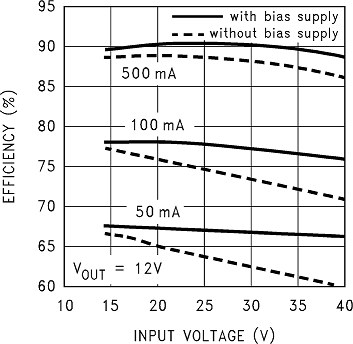 Figure 20. Effects of Bias Supply Feature
on 12-V Regulator Efficiency
8.3.2 SHUTDOWN and Soft-Start
The circuit shown in Figure 23 is a standard buck regulator with 24 VIN, 12 VOUT, 100-mA load, and using a 0.068-μF soft-start capacitor. The photo in Figure 21 and Figure 22 show the effects of soft-start on the output voltage, the input current, with, and without a soft-start capacitor. Figure 21 also shows the error flag output going high when the output voltage reaches 95% of the nominal output voltage. The reduced input current required at start-up is very evident when comparing the two photos. The soft-start feature reduces the start-up current from 700 mA down to 160 mA, and delays and slows down the output voltage rise time.
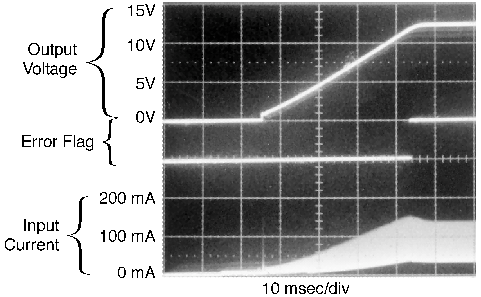 Figure 21. Output Voltage, Input Current,
and Error Flag Signal at Start-Up With Soft-start
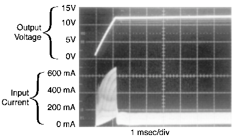 Figure 22. Output Voltage and Input Current
at Start-Up Without Soft-start
This reduction in start-up current is useful in situations where the input power source is limited in the amount of current it can deliver. In some applications, soft start can be used to replace undervoltage lockout or delayed start-up functions.
If a very slow output voltage ramp is desired, the soft-start capacitor can be made much larger. Many seconds or even minutes are possible.
If only the shutdown feature is required, the soft-start capacitor can be eliminated.
 Figure 23. Typical Circuit Using Shutdown/Soft-Start and Error Flag Features
8.3.3 Inverting Regulator
The circuit in Figure 24 converts a positive input voltage to a negative output voltage with a common ground. The circuit operates by bootstrapping the regulators ground pin to the negative output voltage, then grounding the feedback pin, the regulator senses the inverted output voltage and regulates it.
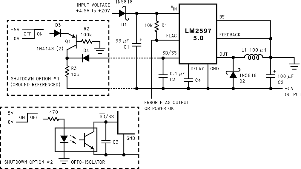 Figure 24. Inverting –5-V Regulator With Shutdown and Soft-Start
This example uses the LM2597-5 to generate a –5-V output, but other output voltages are possible by selecting other output voltage versions, including the adjustable version. Because this regulator topology can produce an output voltage that is either greater than or less than the input voltage, the maximum output current greatly depends on both the input and output voltage. The curve shown in Figure 25 provides a guide as to the amount of output load current possible for the different input and output voltage conditions.
The maximum voltage appearing across the regulator is the absolute sum of the input and output voltage, and this must be limited to a maximum of 40 V. In this example, when converting 20 V to −5 V, the regulator would see 25 V between the input pin and ground pin. The LM2597 has a maximum input voltage rating of 40 V (60 V for the LM2597HV).
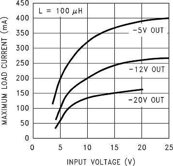 Figure 25. Maximum Load Current for Inverting Regulator Circuit
An additional diode is required in this regulator configuration. Diode D1 is used to isolate input voltage ripple or noise from coupling through the CIN capacitor to the output, under light or no load conditions. Also, this diode isolation changes the topology to closely resemble a buck configuration thus providing good closed loop stability. A Schottky diode is recommended for low input voltages, (because of its lower voltage drop) but for higher input voltages, a 1N4001 diode could be used.
Because of differences in the operation of the inverting regulator, the standard design procedure is not used to select the inductor value. In the majority of designs, a 100-μH, 1-A inductor is the best choice. Capacitor selection can also be narrowed down to just a few values. Using the values shown in Figure 24 will provide good results in the majority of inverting designs.
This type of inverting regulator can require relatively large amounts of input current when starting up, even with light loads. Input currents as high as the LM2597 current limit (approximately 0.8 A) are required for 1 ms or more, until the output reaches its nominal output voltage. The actual time depends on the output voltage and the size of the output capacitor. Input power sources that are current limited or sources that can not deliver these currents without getting loaded down, may not work correctly. Because of the relatively high start-up currents required by the inverting topology, the soft-start feature shown in Figure 24 is recommended.
Also shown in Figure 24 are several shutdown methods for the inverting configuration. With the inverting configuration, some level shifting is required, because the ground pin of the regulator is no longer at ground, but is now at the negative output voltage. The shutdown methods shown accept ground referenced shutdown signals.
8.3.4 Undervoltage Lockout
Some applications require the regulator to remain off until the input voltage reaches a predetermined voltage. Figure 26 shows an undervoltage lockout circuit for a buck configuration, while Figure 27 and Figure 28 are for the inverting types (only the circuitry pertaining to the undervoltage lockout is shown). Figure 26 uses a Zener diode to establish the threshold voltage when the switcher begins operating. When the input voltage is less than the Zener voltage, resistors R1 and R2 hold the Shutdown/Soft-start pin low, keeping the regulator in the shutdown mode. As the input voltage exceeds the Zener voltage, the Zener conducts, pulling the Shutdown/Soft-start pin high, allowing the regulator to begin switching. The threshold voltage for the undervoltage lockout feature is approximately 1.5 V greater than the Zener voltage.
 Figure 26. Undervoltage Lockout for a Buck Regulator
Figure 27 and Figure 28 apply the same feature to an inverting circuit. Figure 27 features a constant threshold voltage for turnon and turnoff (Zener voltage plus approximately 1 V). If hysteresis is required, the circuit in Figure 28 has a turnon voltage which is different than the turnoff voltage. The amount of hysteresis is approximately equal to the value of the output voltage. Since the SD/SS pin has an internal 7-V Zener clamp, R2 is required to limit the current into this pin to approximately 1 mA when Q1 is on.
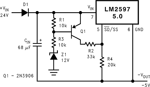 Figure 27. Undervoltage Lockout Without
Hysteresis for an Inverting Regulator
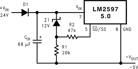 Figure 28. Undervoltage Lockout With
Hysteresis for an Inverting Regulator
8.3.5 Negative Voltage Charge Pump
Occasionally a low current negative voltage is required for biasing parts of a circuit. A simple method of generating a negative voltage using a charge pump technique and the switching waveform present at the OUT pin, is shown in Figure 29. This unregulated negative voltage is approximately equal to the positive input voltage (minus a few volts), and can supply up to a 100 mA of output current. There is a requirement however, that there be a minimum load of several hundred mA on the regulated positive output for the charge pump to work correctly. Also, resistor R1 is required to limit the charging current of C1 to some value less than the LM2597 current limit (typically 800 mA).
This method of generating a negative output voltage without an additional inductor can be used with other members of the SIMPLE SWITCHER family, using either the buck or boost topology.
 Figure 29. Charge Pump for Generating a
Low Current, Negative Output Voltage
8.4 Device Functional Modes
8.4.1 Discontinuous Mode Operation
The selection guide chooses inductor values suitable for continuous mode operation, but for low current applications or high input voltages, a discontinuous mode design may be a better choice. Discontinuous mode would use an inductor that would be physically smaller, and would need only one half to one third the inductance value required for a continuous mode design. The peak switch and inductor currents are higher in a discontinuous design, but at these low load currents (200 mA and below), the maximum switch current will still be less than the switch current limit.
Discontinuous operation can have voltage waveforms that are considerably different than a continuous design. The output pin (switch) waveform can have some damped sinusoidal ringing present. This ringing is normal for discontinuous operation, and is not caused by feedback loop instabilities. In discontinuous operation, there is a period of time where neither the switch nor the diode are conducting, and the inductor current has dropped to zero. During this time, a small amount of energy can circulate between the inductor and the switch and diode parasitic capacitance causing this characteristic ringing. Normally this ringing is not a problem, unless the amplitude becomes great enough to exceed the input voltage, and even then, there is very little energy present to cause damage.
Different inductor types or core materials produce different amounts of this characteristic ringing. Ferrite core inductors have very little core loss and therefore produce the most ringing. The higher core loss of powdered iron inductors produce less ringing. If desired, a series RC could be placed in parallel with the inductor to dampen the ringing.
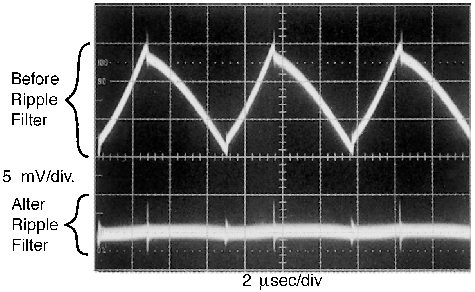 Figure 30. Post Ripple Filter Waveform