SNVS123D April 1998 – May 2016 LM2599
PRODUCTION DATA.
- 1 Features
- 2 Applications
- 3 Description
- 4 Revision History
- 5 Description (continued)
- 6 Pin Configuration and Functions
-
7 Specifications
- 7.1 Absolute Maximum Ratings
- 7.2 ESD Ratings
- 7.3 Recommended Operating Conditions
- 7.4 Thermal Information
- 7.5 Electrical Characteristics - 3.3-V Version
- 7.6 Electrical Characteristics - 5-V Version
- 7.7 Electrical Characteristics - 12-V Version
- 7.8 Electrical Characteristics - Adjustable Voltage Version
- 7.9 Electrical Characteristics - All Output Voltage Versions
- 7.10 Typical Characteristics
- 8 Detailed Description
-
9 Application and Implementation
- 9.1
Application Information
- 9.1.1 Soft-Start Capacitor (CSS)
- 9.1.2 Delay Capacitor (CDELAY)
- 9.1.3 Feedforward Capacitor (CFF) for Adjustable Output Voltage Version Only
- 9.1.4 Input Capacitor (CIN)
- 9.1.5 Output Capacitor (COUT)
- 9.1.6 Catch Diode
- 9.1.7 Inductor Selection
- 9.1.8 Output Voltage Ripple and Transients
- 9.1.9 Open Core Inductors
- 9.2 Typical Applications
- 9.1
Application Information
- 10Power Supply Recommendations
- 11Layout
- 12Device and Documentation Support
- 13Mechanical, Packaging, and Orderable Information
封装选项
机械数据 (封装 | 引脚)
散热焊盘机械数据 (封装 | 引脚)
- KTW|7
订购信息
7 Specifications
7.1 Absolute Maximum Ratings (1)(2)
| MIN | MAX | UNIT | |||
|---|---|---|---|---|---|
| Maximum supply voltage, VIN | 45 | V | |||
| SD/SS pin input voltage(3) | 6 | V | |||
| Delay pin voltage(3) | 1.5 | V | |||
| Flag pin voltage | –0.3 | 45 | V | ||
| Feedback pin voltage | –0.3 | 25 | V | ||
| Output voltage to ground (steady-state) | –1 | V | |||
| Power dissipation | Internally limited | ||||
| Lead temperature | KTW package | Vapor phase (60 s) | 215 | °C | |
| Infrared (10 s) | 245 | ||||
| NDZ package (soldering, 10 s) | 260 | ||||
| Maximum junction temperature | 150 | °C | |||
| Storage temperature, Tstg | −65 | 150 | °C | ||
(1) Stresses beyond those listed under Absolute Maximum Ratings may cause permanent damage to the device. These are stress ratings only, which do not imply functional operation of the device at these or any other conditions beyond those indicated under Recommended Operating Conditions. Exposure to absolute-maximum-rated conditions for extended periods may affect device reliability.
(2) If Military/Aerospace specified devices are required, please contact the Texas Instruments Sales Office/Distributors for availability and specifications.
(3) Voltage internally clamped. If clamp voltage is exceeded, limit current to a maximum of 1 mA.
7.2 ESD Ratings
| VALUE | UNIT | |||
|---|---|---|---|---|
| V(ESD) | Electrostatic discharge | Human-body model (HBM), per ANSI/ESDA/JEDEC JS-001(1) | ±2000 | V |
(1) JEDEC document JEP155 states that 500-V HBM allows safe manufacturing with a standard ESD control process.
7.3 Recommended Operating Conditions
| MIN | MAX | UNIT | |
|---|---|---|---|
| Supply voltage | 4.5 | 40 | V |
| Temperature | –40 | 125 | °C |
7.4 Thermal Information
| THERMAL METRIC(1) | LM2599 | UNIT | |||
|---|---|---|---|---|---|
| KTW (TO-263) | NDZ (TO-220) | ||||
| 7 PINS | 7 PINS | ||||
| RθJA | Junction-to-ambient thermal resistance(2)(3) | See(4) | — | 50 | °C/W |
| See(5) | 50 | — | |||
| See(6) | 30 | — | |||
| See(7) | 20 | — | |||
| RθJC(top) | Junction-to-case (top) thermal resistance | 2 | 2 | °C/W | |
(1) For more information about traditional and new thermal metrics, see the Semiconductor and IC Package Thermal Metrics application report, SPRA953.
(2) The package thermal impedance is calculated in accordance to JESD 51-7.
(3) Thermal resistances were simulated on a 4-layer, JEDEC board.
(4) Junction to ambient thermal resistance (no external heat sink) for the package mounted TO-220 package mounted vertically, with the leads soldered to a PCB with 1-oz copper area of approximately 1 in2.
(5) Junction to ambient thermal resistance with the TO-263 package tab soldered to a single-sided PCB with 0.5 in2 of 1-oz copper area.
(6) Junction to ambient thermal resistance with the TO-263 package tab soldered to a single-sided PCB with 2.5 in2 of 1-oz copper area.
(7) Junction to ambient thermal resistance with the TO-263 package tab soldered to a double-sided PCB with 3 in2 of 1-oz copper area on the LM2599S side of the board, and approximately 16 in2 of copper on the other side of the PCB.
7.5 Electrical Characteristics – 3.3-V Version
Specifications are for TJ = 25°C (unless otherwise noted).| PARAMETER | TEST CONDITIONS | MIN(1) | TYP(2) | MAX (1) | UNIT | ||
|---|---|---|---|---|---|---|---|
| SYSTEM PARAMETERS(3) (see Figure 43 for test circuit) | |||||||
| VOUT | Output voltage | 4.75 V ≤ VIN ≤ 40 V, 0.2 A ≤ ILOAD ≤ 3 A |
TJ = 25°C | 3.168 | 3.3 | 3.432 | V |
| –40°C ≤ TJ ≤ 125°C | 3.135 | 3.465 | |||||
| η | Efficiency | VIN = 12 V, ILOAD = 3 A | 73% | ||||
(1) All room temperature limits are 100% production tested. All limits at temperature extremes are specified via correlation using standard Statistical Quality Control (SQC) methods. All limits are used to calculate Average Outgoing Quality Level (AOQL).
(2) Typical numbers are at 25°C and represent the most likely norm.
(3) External components such as the catch diode, inductor, input and output capacitors can affect switching regulator system performance. When the LM2599 is used as shown in Figure 43, system performance is shown in the test conditions column.
7.6 Electrical Characteristics – 5-V Version
Specifications are for TJ = 25°C (unless otherwise noted).| PARAMETER | TEST CONDITIONS | MIN(1) | TYP(2) | MAX(1) | UNIT | ||
|---|---|---|---|---|---|---|---|
| SYSTEM PARAMETERS(3) (see Figure 43 for test circuit) | |||||||
| VOUT | Output voltage | 7 V ≤ VIN ≤ 40 V, 0.2 A ≤ ILOAD ≤ 3 A |
TJ = 25°C | 4.8 | 5 | 5.2 | V |
| –40°C ≤ TJ ≤ 125°C | 4.75 | 5.25 | |||||
| η | Efficiency | VIN = 12 V, ILOAD = 3 A | 80% | ||||
(1) All room temperature limits are 100% production tested. All limits at temperature extremes are specified via correlation using standard Statistical Quality Control (SQC) methods. All limits are used to calculate Average Outgoing Quality Level (AOQL).
(2) Typical numbers are at 25°C and represent the most likely norm.
(3) External components such as the catch diode, inductor, input and output capacitors can affect switching regulator system performance. When the LM2599 is used as shown in Figure 43, system performance is shown in the test conditions column.
7.7 Electrical Characteristics – 12-V Version
Specifications are for TJ = 25°C (unless otherwise noted).| PARAMETER | TEST CONDITIONS | MIN(1) | TYP(2) | MAX(1) | UNIT | ||
|---|---|---|---|---|---|---|---|
| SYSTEM PARAMETERS(3) (see Figure 43 for test circuit) | |||||||
| VOUT | Output voltage | 15 V ≤ VIN ≤ 40 V, 0.2 A ≤ ILOAD ≤ 3 A |
TJ = 25°C | 11.52 | 12 | 12.48 | V |
| –40°C ≤ TJ ≤ 125°C | 11.4 | 12.6 | |||||
| η | Efficiency | VIN = 25 V, ILOAD = 3 A | 90% | ||||
(1) All room temperature limits are 100% production tested. All limits at temperature extremes are specified via correlation using standard Statistical Quality Control (SQC) methods. All limits are used to calculate Average Outgoing Quality Level (AOQL).
(2) Typical numbers are at 25°C and represent the most likely norm.
(3) External components such as the catch diode, inductor, input and output capacitors can affect switching regulator system performance. When the LM2599 is used as shown in Figure 43, system performance is shown in the test conditions column.
7.8 Electrical Characteristics – Adjustable Voltage Version
Specifications are for TJ = 25°C (unless otherwise noted).| PARAMETER | TEST CONDITIONS | MIN(1) | TYP(2) | MAX(1) | UNIT | ||
|---|---|---|---|---|---|---|---|
| SYSTEM PARAMETERS(3) (see Figure 43 for test circuit) | |||||||
| VFB | Feedback voltage | 4.5 V ≤ VIN ≤ 40 V, 0.2 A ≤ ILOAD ≤ 3 A | 1.23 | V | |||
| VOUT programmed for 3 V, circuit of Figure 43 |
TJ = 25°C | 1.193 | 1.267 | ||||
| –40°C ≤ TJ ≤ 125°C | 1.18 | 1.28 | |||||
| η | Efficiency | VIN = 12 V, VOUT = 3 V, ILOAD = 3 A | 73% | ||||
(1) All room temperature limits are 100% production tested. All limits at temperature extremes are specified via correlation using standard Statistical Quality Control (SQC) methods. All limits are used to calculate Average Outgoing Quality Level (AOQL).
(2) Typical numbers are at 25°C and represent the most likely norm.
(3) External components such as the catch diode, inductor, input and output capacitors can affect switching regulator system performance. When the LM2599 is used as shown in Figure 43, system performance is shown in the test conditions column.
7.9 Electrical Characteristics – All Output Voltage Versions
Specifications are for TJ = 25°C, ILOAD = 500 mA, VIN = 12 V for the 3.3-V, 5-V, and Adjustable version, and VIN = 24 V for the 12-V version (unless otherwise noted).| PARAMETER | TEST CONDITIONS | MIN(1) | TYP(2) | MAX(1) | UNIT | ||
|---|---|---|---|---|---|---|---|
| DEVICE PARAMETERS | |||||||
| Ib | Feedback bias current | Adjustable voltage version only, VFB = 1.3 V | TJ = 25°C | 10 | 50 | nA | |
| –40°C ≤ TJ ≤ 125°C | 100 | ||||||
| fO | Oscillator frequency(3) | TJ = 25°C | 127 | 150 | 173 | kHz | |
| –40°C ≤ TJ ≤ 125°C | 110 | 173 | |||||
| VSAT | Saturation voltage | IOUT = 3 A(4)(5) | TJ = 25°C | 1.16 | 1.4 | V | |
| –40°C ≤ TJ ≤ 125°C | 1.5 | ||||||
| DC | Max duty cycle (ON)(5) | 100% | |||||
| Min duty cycle (OFF)(6) | 0% | ||||||
| ICL | Current limit | Peak current(4) (5) | TJ = 25°C | 3.6 | 4.5 | 6.9 | A |
| –40°C ≤ TJ ≤ 125°C | |||||||
| 3.4 | 7.5 | ||||||
| IL | Output leakage current | Output = 0 V, VIN = 40 V(4) (6) | 50 | μA | |||
| Output = −1 V | 2 | 30 | mA | ||||
| IQ | Operating quiescent current | SD/SS pin open(6) | 5 | 10 | mA | ||
| ISTBY | Current standby quiescent | SD/SS pin = 0 V, VIN = 40 V | TJ = 25°C | 80 | 200 | μA | |
| –40°C ≤ TJ ≤ 125°C | 250 | μA | |||||
| SHUTDOWN/SOFT-START CONTROL – See Figure 43 | |||||||
| VSD | Shutdown threshold voltage | 1.3 | V | ||||
| Low (Shutdown mode), –40°C ≤ TJ ≤ 125°C | 0.6 | ||||||
| High (Soft-start mode), –40°C ≤ TJ ≤ 125°C | 2 | ||||||
| VSS | Soft-start voltage | VOUT = 20% of nominal output voltage | 2 | V | |||
| VOUT = 100% of nominal output voltage | 3 | ||||||
| ISD | Shutdown current | VSHUTDOWN = 0.5 V | 5 | 10 | μA | ||
| ISS | Soft-start current | VSoft-start = 2.5 V | 1.6 | 5 | μA | ||
| FLAG/DELAY CONTROL – See Figure 43 | |||||||
| Regulator dropout detector threshold voltage | Low (flag ON) | 92% | 96% | 98% | |||
| VFSAT | Voltage flag output saturation | ISINK = 3 mA | 0.3 | V | |||
| VDELAY = 0.5 V | TJ = 25°C | 0.7 | V | ||||
| –40°C ≤ TJ ≤ 125°C | 1 | ||||||
| IFL | Flag output leakage current | VFLAG = 40 V | 0.3 | μA | |||
| Voltage delay pin threshold | 1.25 | V | |||||
| Low (flag ON) | 1.21 | V | |||||
| High (flag OFF) and VOUT regulated | 1.29 | ||||||
| Delay pin source current | VDELAY = 0.5 V | 3 | 6 | μA | |||
| Delay pin saturation | Low (flag ON) | TJ = 25°C | 55 | 350 | mV | ||
| –40°C ≤ TJ ≤ 125°C | 400 | ||||||
(1) All room temperature limits are 100% production tested. All limits at temperature extremes are specified via correlation using standard Statistical Quality Control (SQC) methods. All limits are used to calculate Average Outgoing Quality Level (AOQL).
(2) Typical numbers are at 25°C and represent the most likely norm.
(3) The switching frequency is reduced when the second stage current limit is activated. The amount of reduction is determined by the severity of current overload.
(4) No diode, inductor or capacitor connected to output pin.
(5) Feedback pin removed from output and connected to 0 V to force the output transistor switch ON.
(6) Feedback pin removed from output and connected to 12 V for the 3.3-V, 5-V, and the adjustable versions, and 15 V for the 12-V version, to force the output transistor switch OFF.
7.10 Typical Characteristics
See Figure 43 for test circuit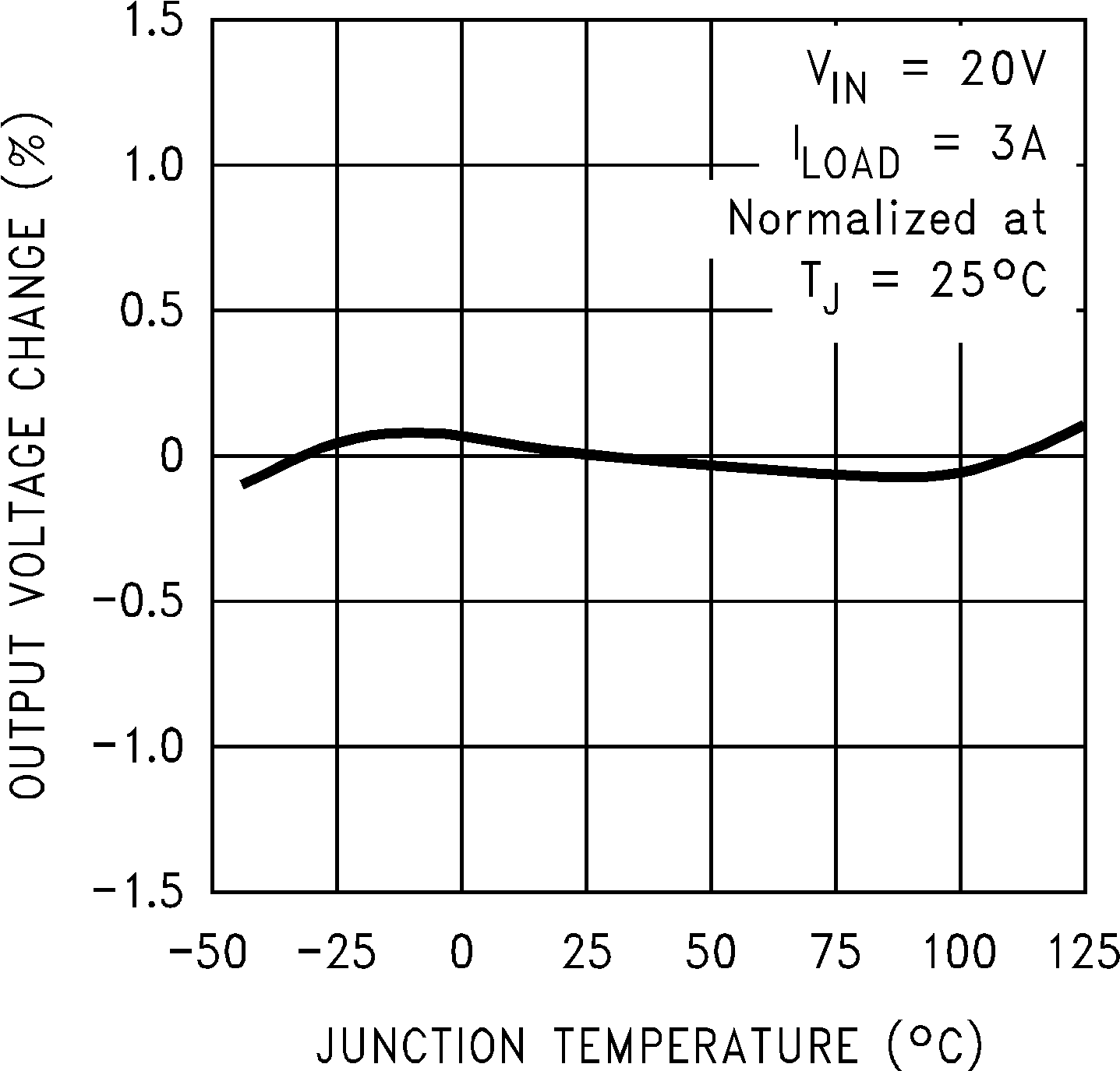 Figure 1. Normalized Output Voltage
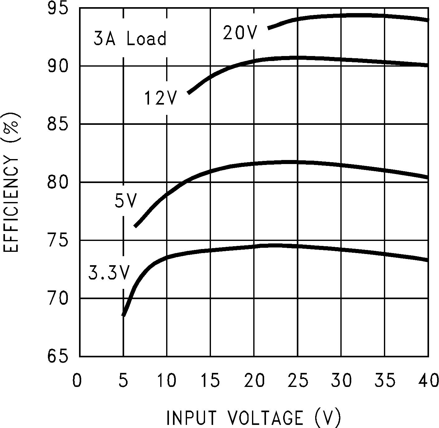 Figure 3. Efficiency
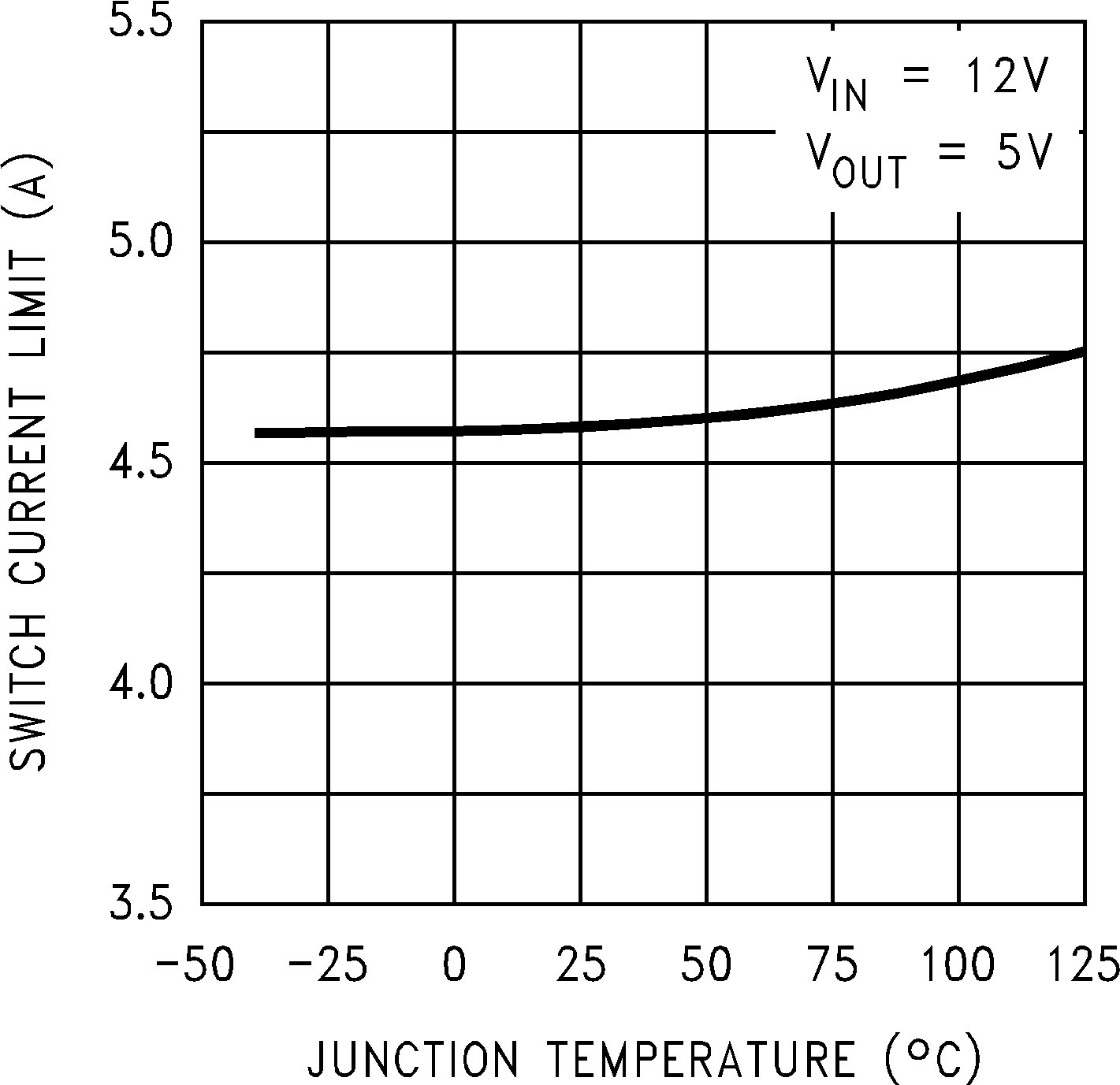 Figure 5. Switch Current Limit
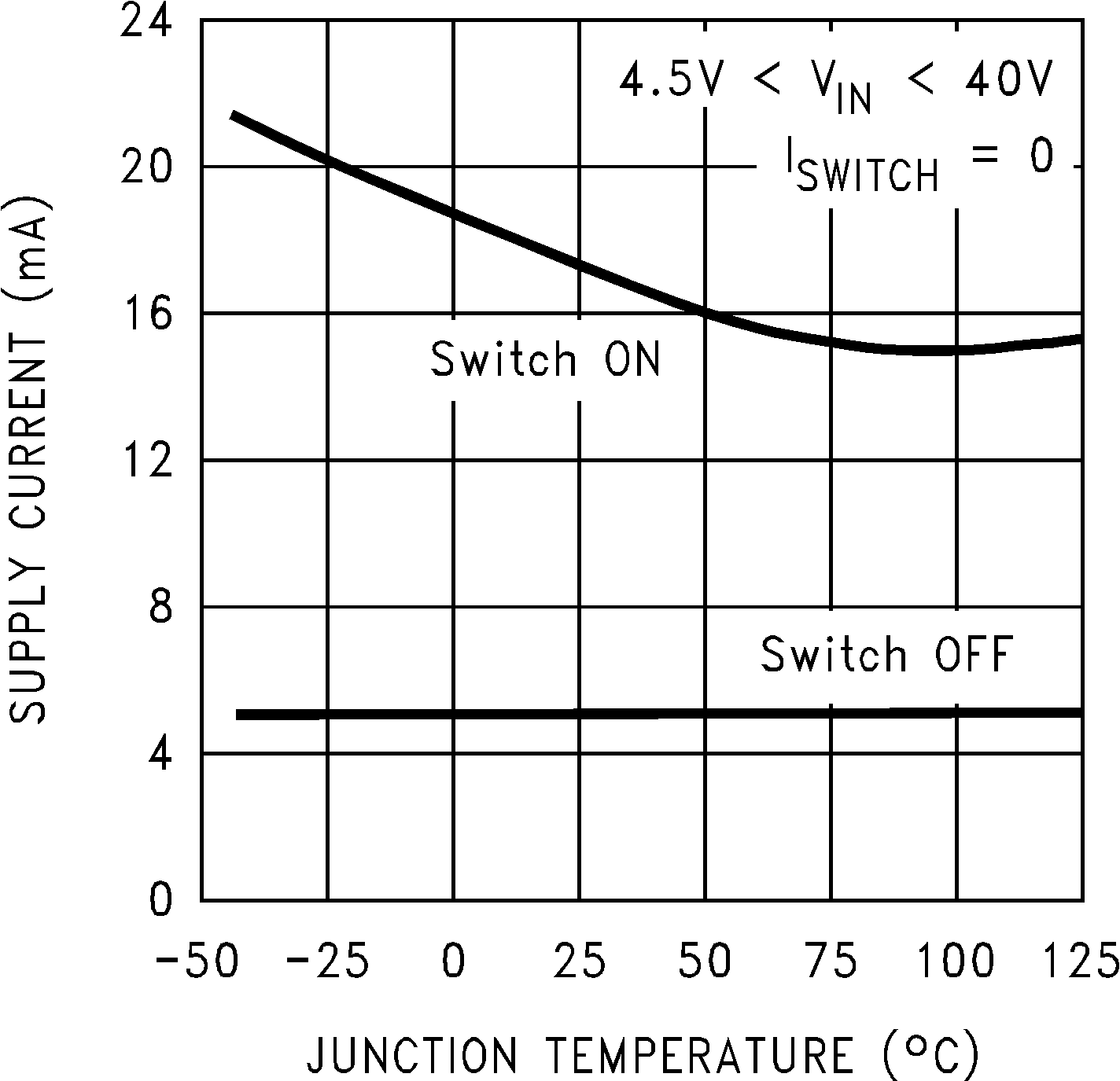 Figure 7. Operating Quiescent Current
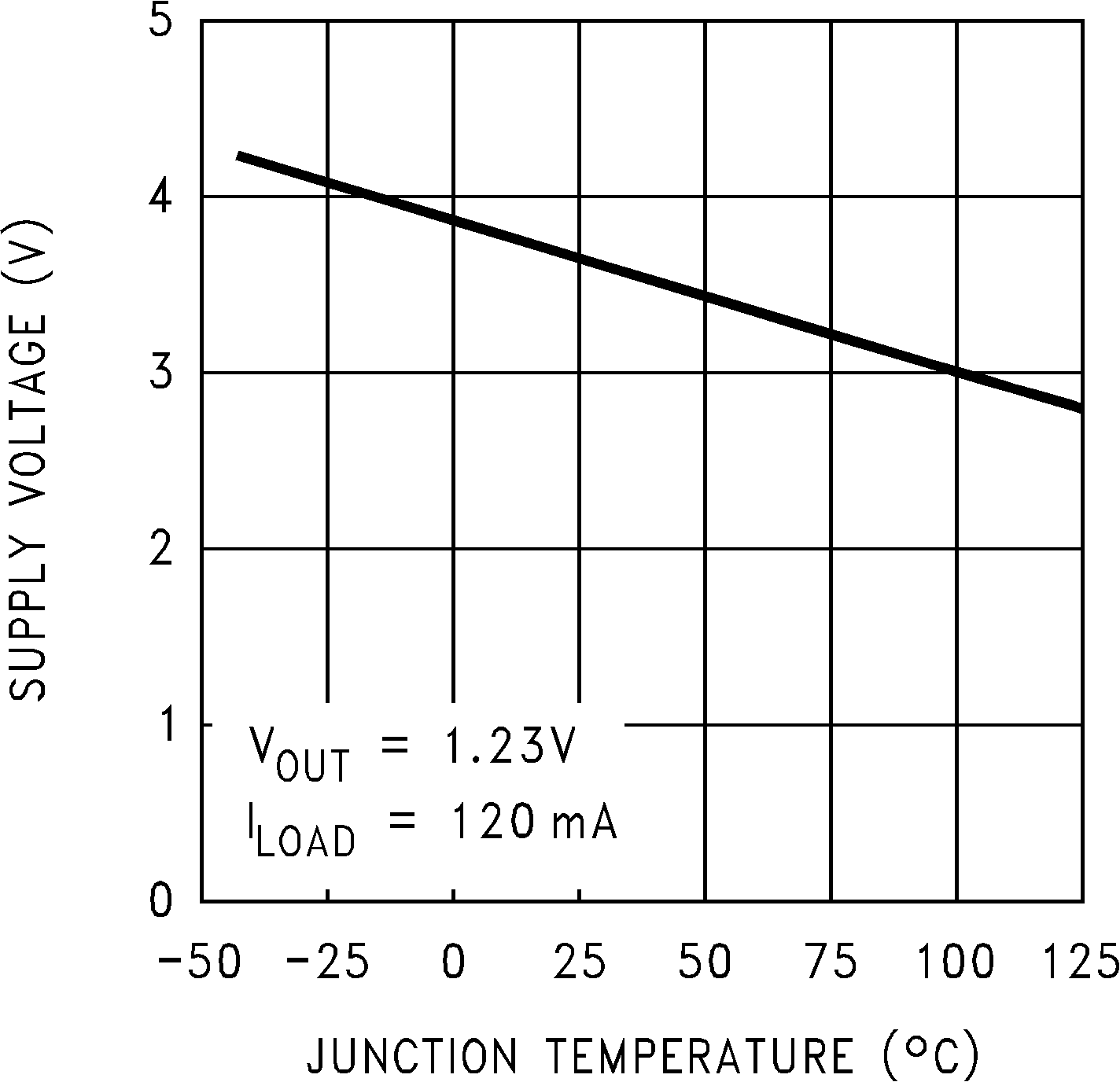 Figure 9. Minimum Operating Supply Voltage
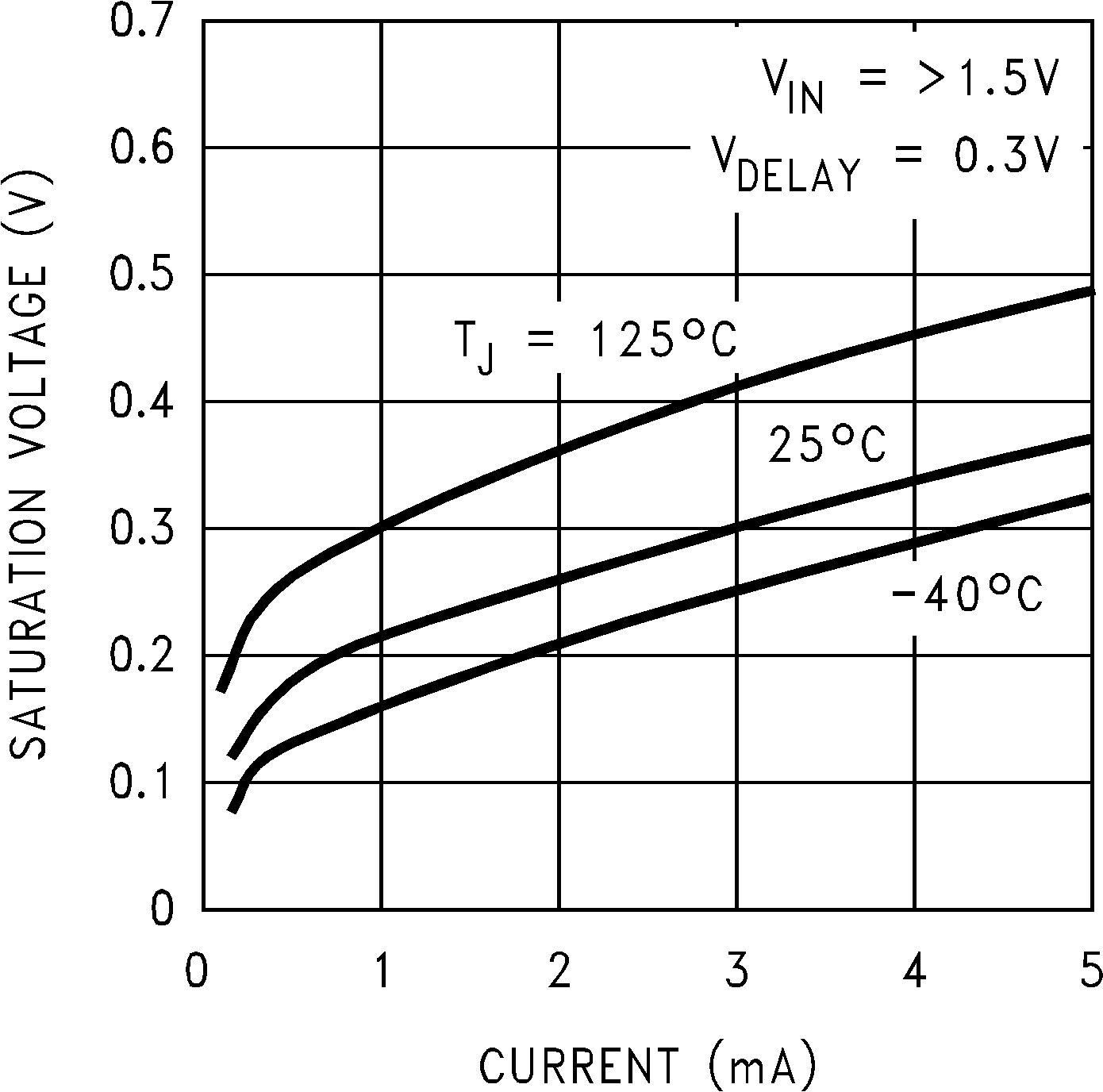 Figure 11. Flag Saturation Voltage
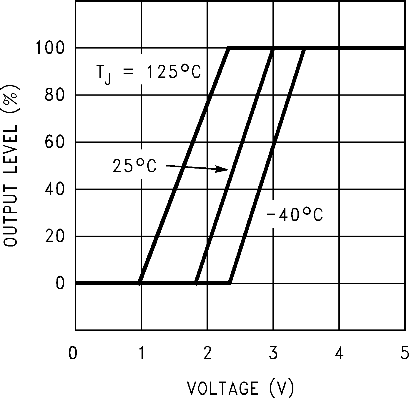 Figure 13. Soft-Start
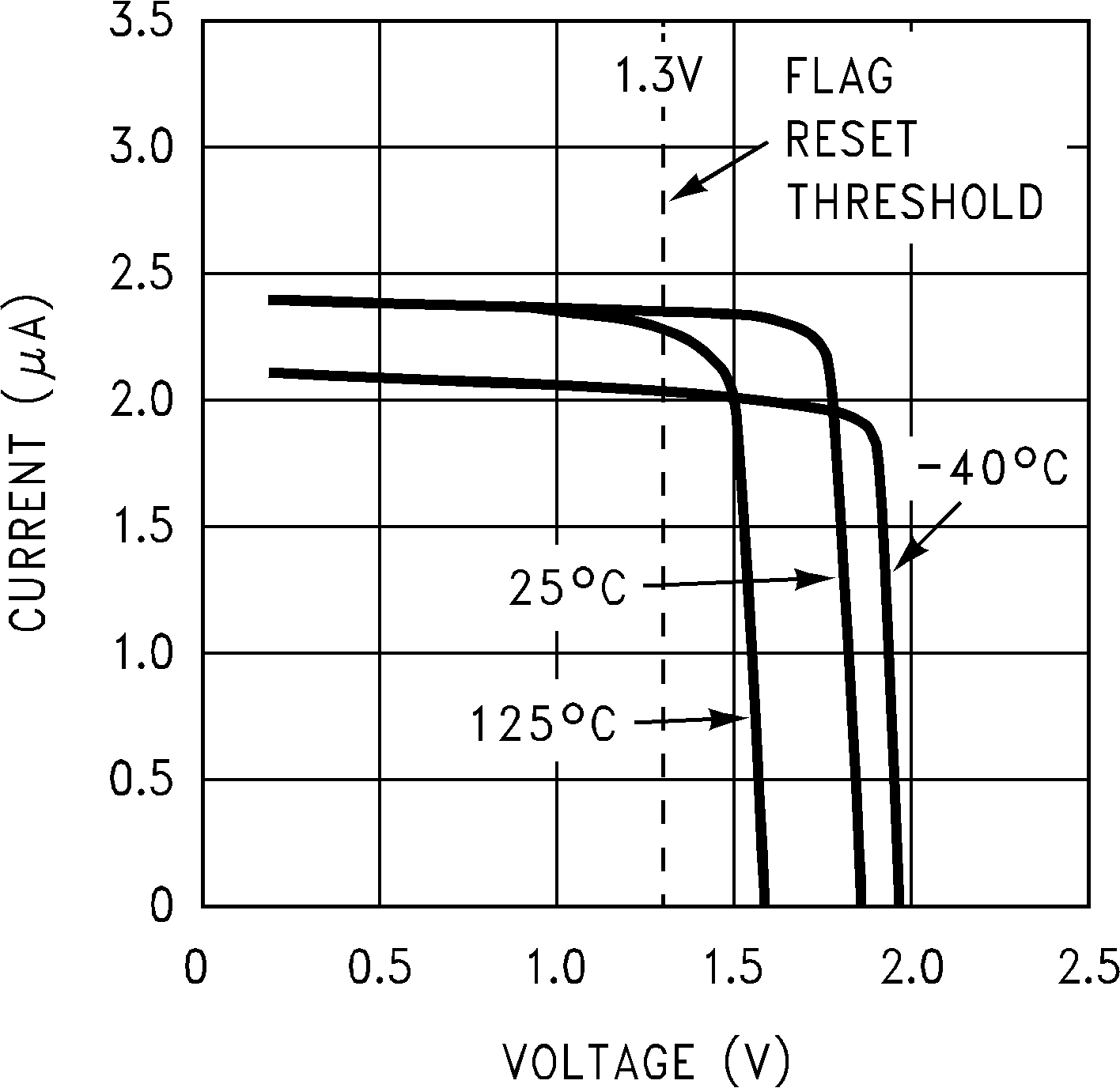 Figure 15. Daisy Pin Current
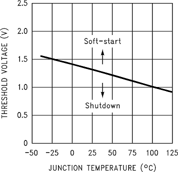 Figure 17. Shutdown/Soft-Start Threshold Voltage
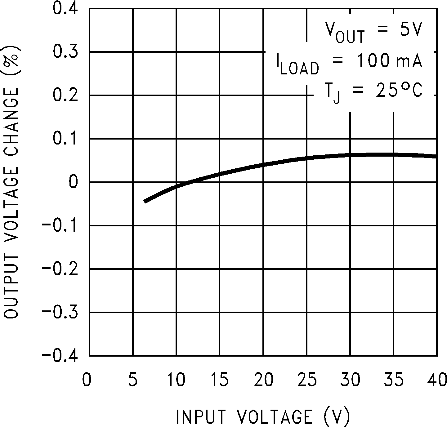 Figure 2. Line Regulation
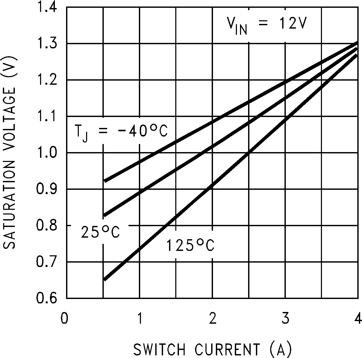 Figure 4. Switch Saturation Voltage
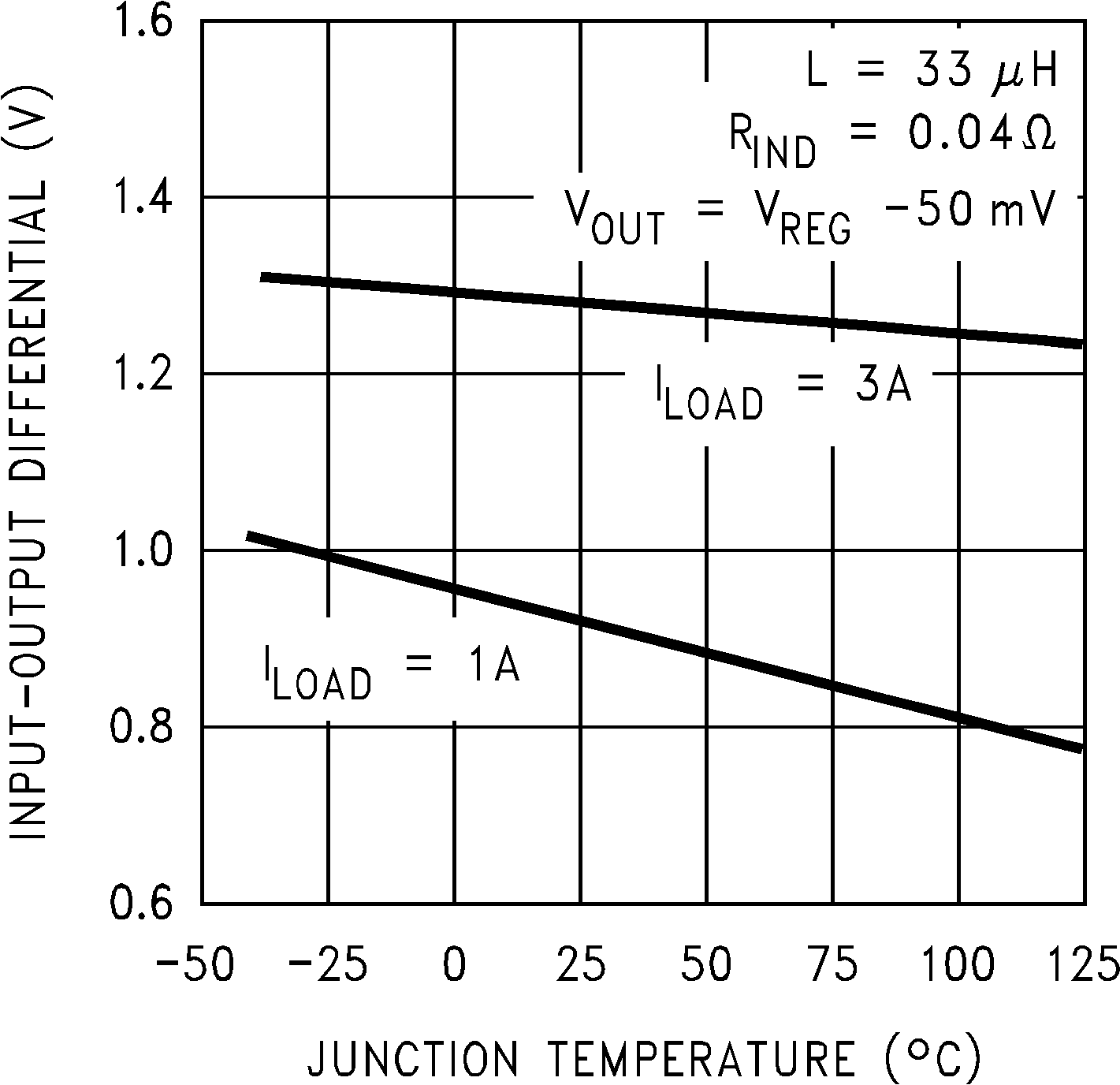 Figure 6. Dropout Voltage
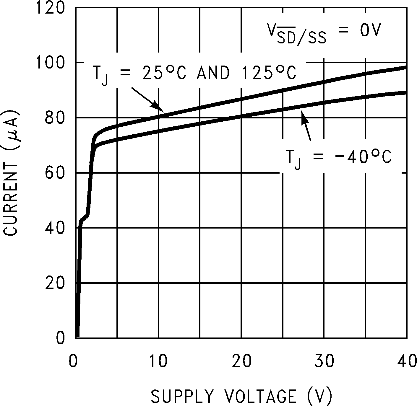 Figure 8. Shutdown Quiescent Current
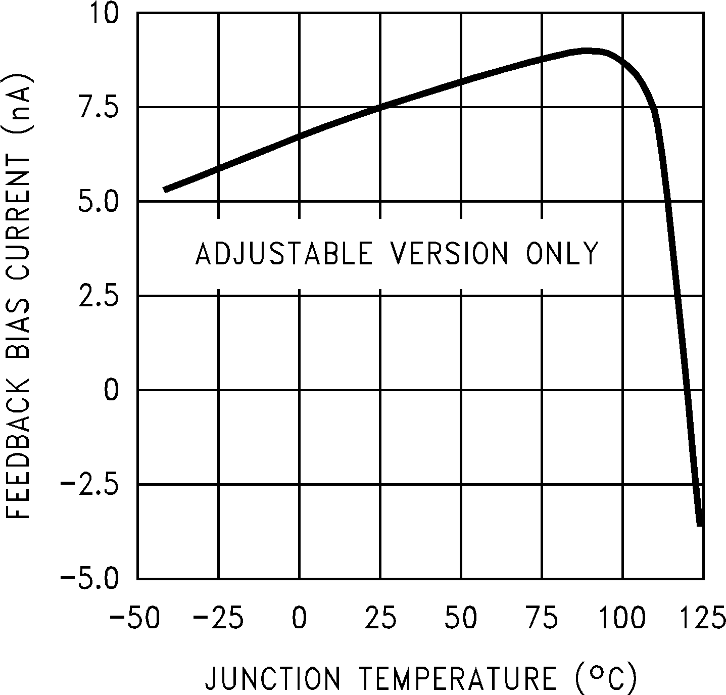 Figure 10. Feedback Pin Bias Current
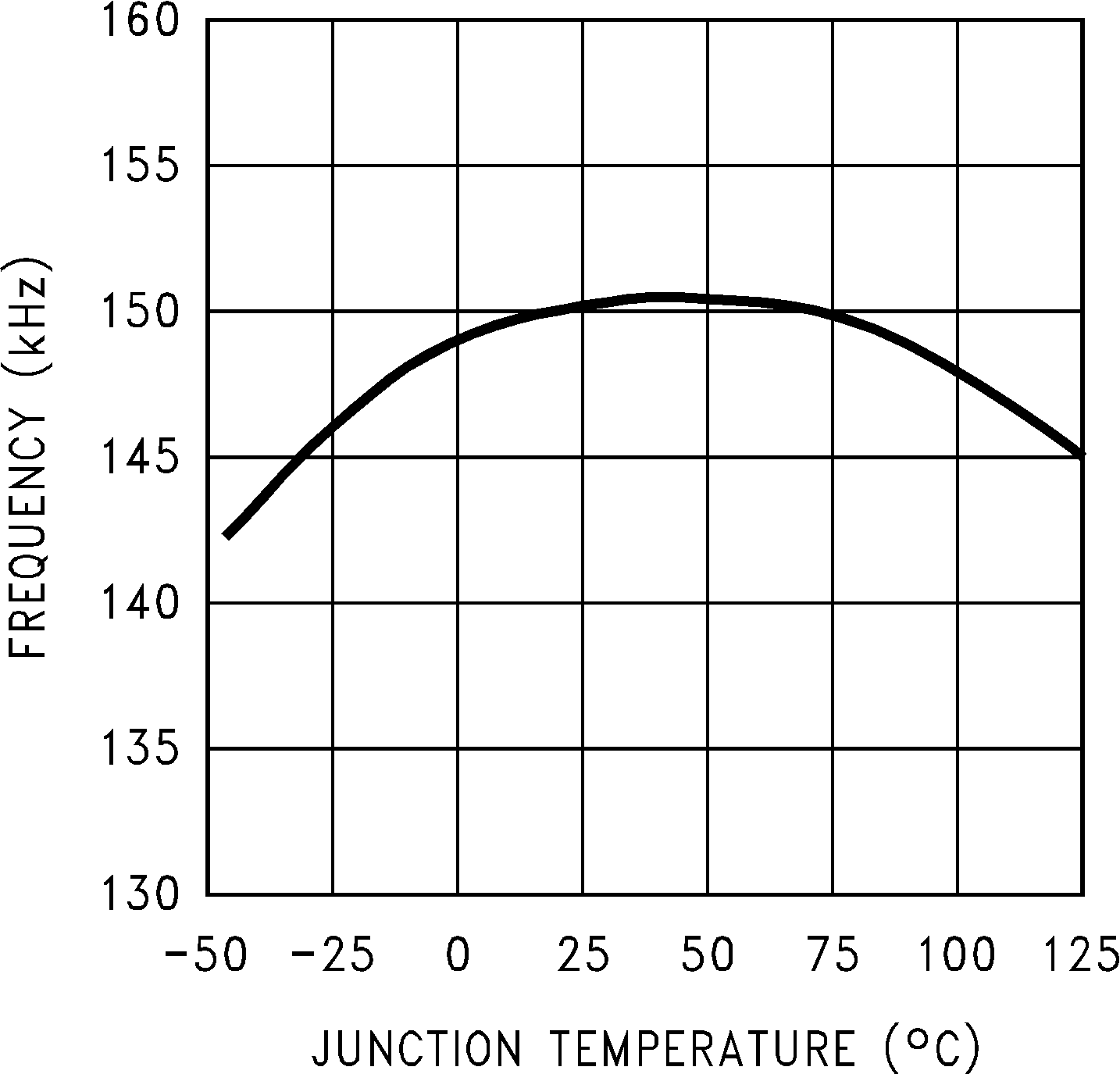 Figure 12. Switching Frequency
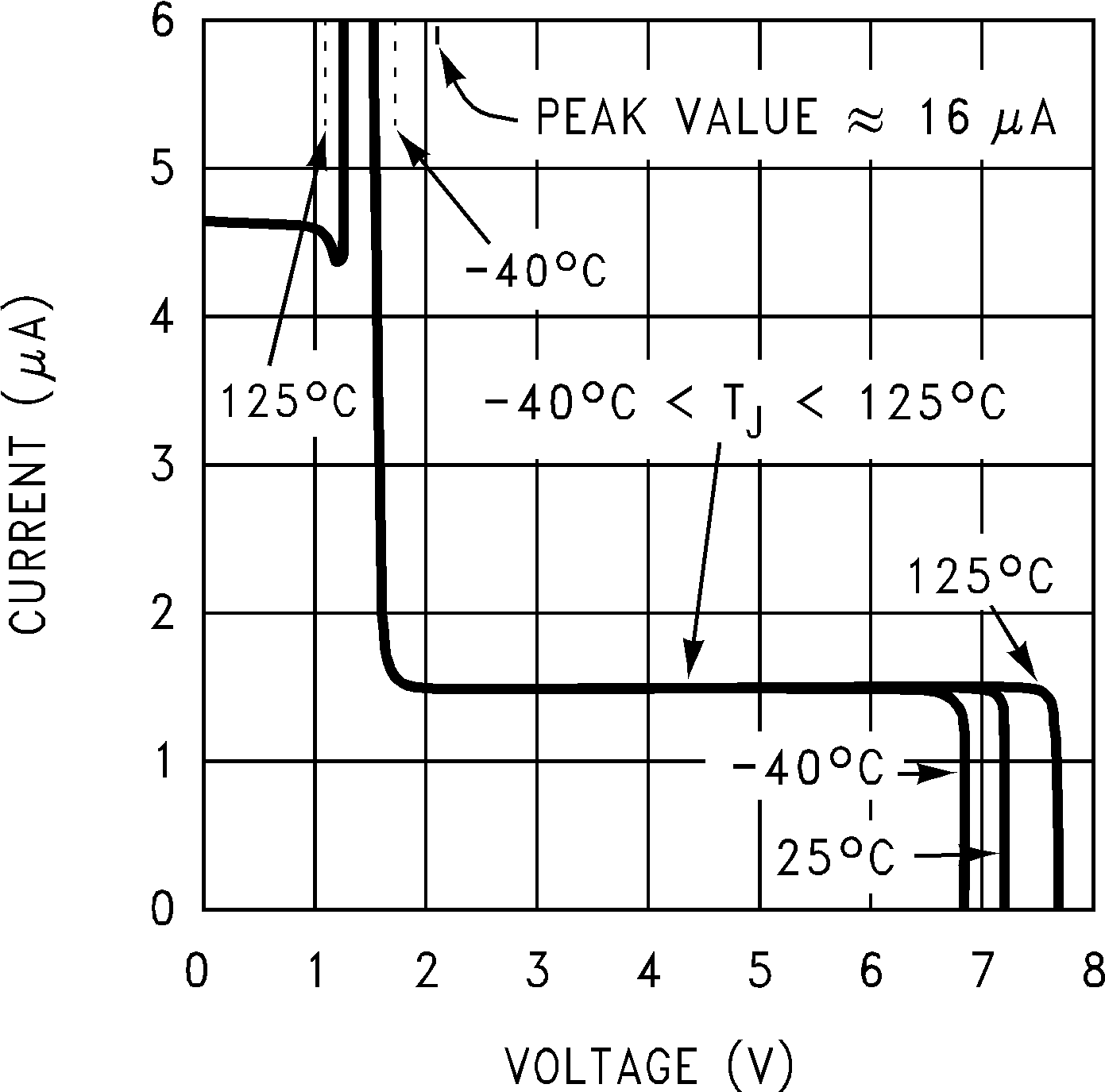 Figure 14. Shutdown/Soft-Start Current
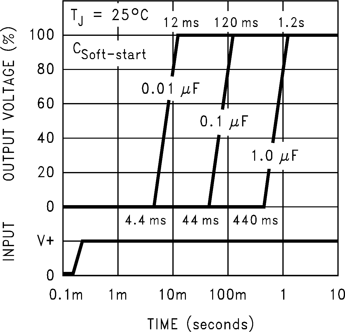 Figure 16. Soft-Start Response