SNVS188I May 2004 – October 2017 LM2623
PRODUCTION DATA.
- 1 Features
- 2 Applications
- 3 Description
- 4 Revision History
- 5 Pin Configuration And Functions
- 6 Specifications
- 7 Detailed Description
- 8 Applications And Implementation
- 9 Power Supply Recommendations
- 10Layout
- 11Device And Documentation Support
- 12Mechanical, Packaging, And Orderable Information
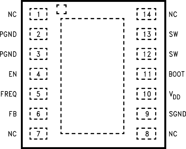
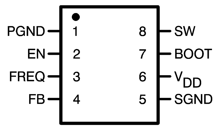
5 Pin Configuration And Functions
NHE Package
14-Pin WSON
Top View

DGK Package
8-Pin VSSOP
Top View

Pin Functions
| PIN | TYPE | DESCRIPTION | |||
|---|---|---|---|---|---|
| WSON | VSSOP | NAME | |||
| 1 | — | NC | N/A | No Connect | |
| 2, 3 | 1 | PGND | GND | Power Ground (WSON Pins 2 and 3 must be shorted together). | |
| 4 | 2 | EN | Digital | Active-Low Shutdown Input | |
| 5 | 3 | FREQ | Analog | Frequency Adjust. An external resistor connected between this pin and a voltage source sets the switching frequency of the LM2623. | |
| 6 | 4 | FB | Analog | Output Voltage Feedback | |
| 7 | — | NC | N/A | No Connect | |
| 8 | — | NC | N/A | No connect | |
| 9 | 5 | SGND | GND | Signal Ground | |
| 10 | 6 | VDD | Power | Power Supply for Internal Circuitry | |
| 11 | 7 | BOOT | Analog | Bootstrap Supply for the Gate Drive of Internal MOSFET Power Switch | |
| 12, 13 | 8 | SW | Analog | Drain of the Internal MOSFET Power Switch. (WSON pins 12 and 13 must be shorted together.) | |
| 14 | — | NC | N/A | No Connect | |
| DAP | — | DAP | Thermal | To be soldered to board for enhanced thermal dissipation. To be electrically isolated/floating. | |