SNVS188I May 2004 – October 2017 LM2623
PRODUCTION DATA.
- 1 Features
- 2 Applications
- 3 Description
- 4 Revision History
- 5 Pin Configuration And Functions
- 6 Specifications
- 7 Detailed Description
- 8 Applications And Implementation
- 9 Power Supply Recommendations
- 10Layout
- 11Device And Documentation Support
- 12Mechanical, Packaging, And Orderable Information
6 Specifications
6.1 Absolute Maximum Ratings(1)(2)
| MIN | MAX | UNIT | |
|---|---|---|---|
| SW pin voltage | –0.5 | 14.5 | V |
| BOOT, VDD, EN and FB pins | –0.5 | 10 | V |
| FREQ pin | 100 | µA | |
| TJmax(3) | 150 | °C | |
| Lead temp. (soldering, 5 sec) | 260 | °C | |
| Power dissipation (TA=25°C)(3) | 500 | mW | |
| Storage temperature, Tstg | –65 | 150 | °C |
(1) Stresses beyond those listed under Absolute Maximum Ratings may cause permanent damage to the device. These are stress ratings only, which do not imply functional operation of the device at these or any other conditions beyond those indicated under Recommended Operating Conditions. Exposure to absolute-maximum-rated conditions for extended periods may affect device reliability.
(2) If Military/Aerospace specified devices are required, contact the Texas Instruments Sales Office/ Distributors for availability and specifications.
(3) The maximum power dissipation must be derated at elevated temperatures and is dictated by Tjmax (maximum junction temperature), RθJA (junction-to-ambient thermal resistance), and TA (ambient temperature). The maximum allowable power dissipation at any temperature is Pdmax = (Tjmax – TA) / RθJA or the number given in the Absolute Maximum Ratings, whichever is lower.
6.2 ESD Ratings
| VALUE | UNIT | ||||
|---|---|---|---|---|---|
| V(ESD) | Electrostatic discharge | Human-body model (HBM), per ANSI/ESDA/JEDEC JS-001(1) | All pins except SW pin | ±2000 | V |
| SW pin (VSSOP package pin 8) (WSON package pin 12 and pin 13) | ±1000 | ||||
| Charged-device model (CDM), per JEDEC specification JESD22-C101(2) | All pins | ±500 | |||
(1) JEDEC document JEP155 states that 500-V HBM allows safe manufacturing with a standard ESD control process.
(2) JEDEC document JEP157 states that 250-V CDM allows safe manufacturing with a standard ESD control process.
6.3 Recommended Operating Conditions
over operating free-air temperature range (unless otherwise noted)(1)| MIN | MAX | UNIT | |
|---|---|---|---|
| VDD pin | 3 | 5 | V |
| FB, EN pins | 0 | VDD | |
| BOOT pin | 0 | 10 | V |
| Ambient temperature (TA) | −40 | 85 | °C |
(1) Stresses beyond those listed under Absolute Maximum Ratings may cause permanent damage to the device. These are stress ratings only, which do not imply functional operation of the device at these or any other conditions beyond those indicated under Recommended Operating Conditions. Exposure to absolute-maximum-rated conditions for extended periods may affect device reliability.
6.4 Thermal Information
| THERMAL METRIC(1) | LM2623 | UNIT | ||
|---|---|---|---|---|
| NHE (WSON) | DGK (VSSOP | |||
| 14 PINS | 8 PINS | |||
| RθJA | Junction-to-ambient thermal resistance | 46.5 | 152.5 | °C/W |
| RθJC(top) | Junction-to-case (top) thermal resistance | 37.7 | 53.9 | °C/W |
| RθJB | Junction-to-board thermal resistance | 23.6 | 73.2 | °C/W |
| ψJT | Junction-to-top characterization parameter | 0.4 | 5.5 | °C/W |
| ψJB | Junction-to-board characterization parameter | 23.8 | 72.0 | °C/W |
| RθJC(bot) | Junction-to-case (bottom) thermal resistance | 4.6 | N/A | °C/W |
(1) For more information about traditional and new thermal metrics, see the Semiconductor and IC Package Thermal Metrics application report.
6.5 Electrical Characteristics
Limits apply for TJ = 25°C and VDD = VOUT = 3.3 V, unless otherwise specified.| PARAMETER | TEST CONDITION | MIN | TYP | MAX | UNIT | |
|---|---|---|---|---|---|---|
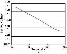
| VDD_ST | Start-up supply voltage 25°C | ILOAD = 0 mA(1) | 1.1 | V | ||
| VIN_OP | Minimum operating supply voltage (once started) | ILOAD = 0 mA | 0.65 | 0.8 | V | |
| VFB | FB pin voltage | 1.24 | V | |||
| −40°C to 85°C | 1.2028 | 1.2772 | ||||
| VOUT_MAX | Maximum output voltage | 14 | V | |||
| η | Efficiency | VIN = 3.6 V; VOUT = 5 V; ILOAD = 500 mA |
87% | |||
| VIN = 2.5 V; VOUT = 3.3 V; ILOAD = 200 mA |
87% | |||||
| D | Switch duty cycle | 17 | ||||
| IDD | Operating quiescent current(2) | FB Pin > 1.3 V; EN Pin at VDD | 80 | µA | ||
| FB Pin > 1.3 V; EN Pin at VDD, −40°C to 85°C | 110 | |||||
| ISD | Shutdown quiescent current(3) | VDD, BOOT and SW Pins at 5 V; EN Pin < 200 mV |
0.01 | µA | ||
| VDD, BOOT and SW Pins at 5 V; EN Pin < 200 mV, −40°C to 85°C |
2.5 | |||||
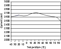
| ICL | Switch peak current limit | LM2623A | 2.2 | 2. 85 | A | |
| IC | Switch peak current limit | LM2623 | 1.2 | |||
| RDS_ON | MOSFET switch on resistance | 0.17 | Ω | |||
| −40°C to 85°C | 0.26 | |||||
| ENABLE SECTION | ||||||
| VEN_LO | EN pin voltage low(4) | −40°C to 85°C | 0.15 VDD | V | ||
| VEN_HI | EN pin voltage high(4) | −40°C to 85°C | 0.7 VDD | |||
(1) VDD tied to BOOT and EN pins. Frequency pin tied to VDD through 121-KΩ resistor. VDD_ST = VDD when start-up occurs. VIN is VDD + D1 voltage (usually 10 mV to 50 mV at start-up).
(2) This is the current into the VDD pin.
(3) This is the total current into pins VDD, BOOT, SW, and FREQ.
(4) When the EN pin is below VEN_LO, the regulator is shut down; when it is above VEN_HI, the regulator is operating.
6.6 Typical Characteristics
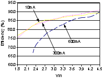
| VOUT = 5 V |
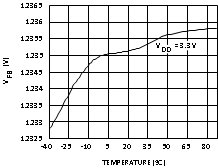
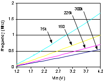
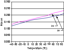
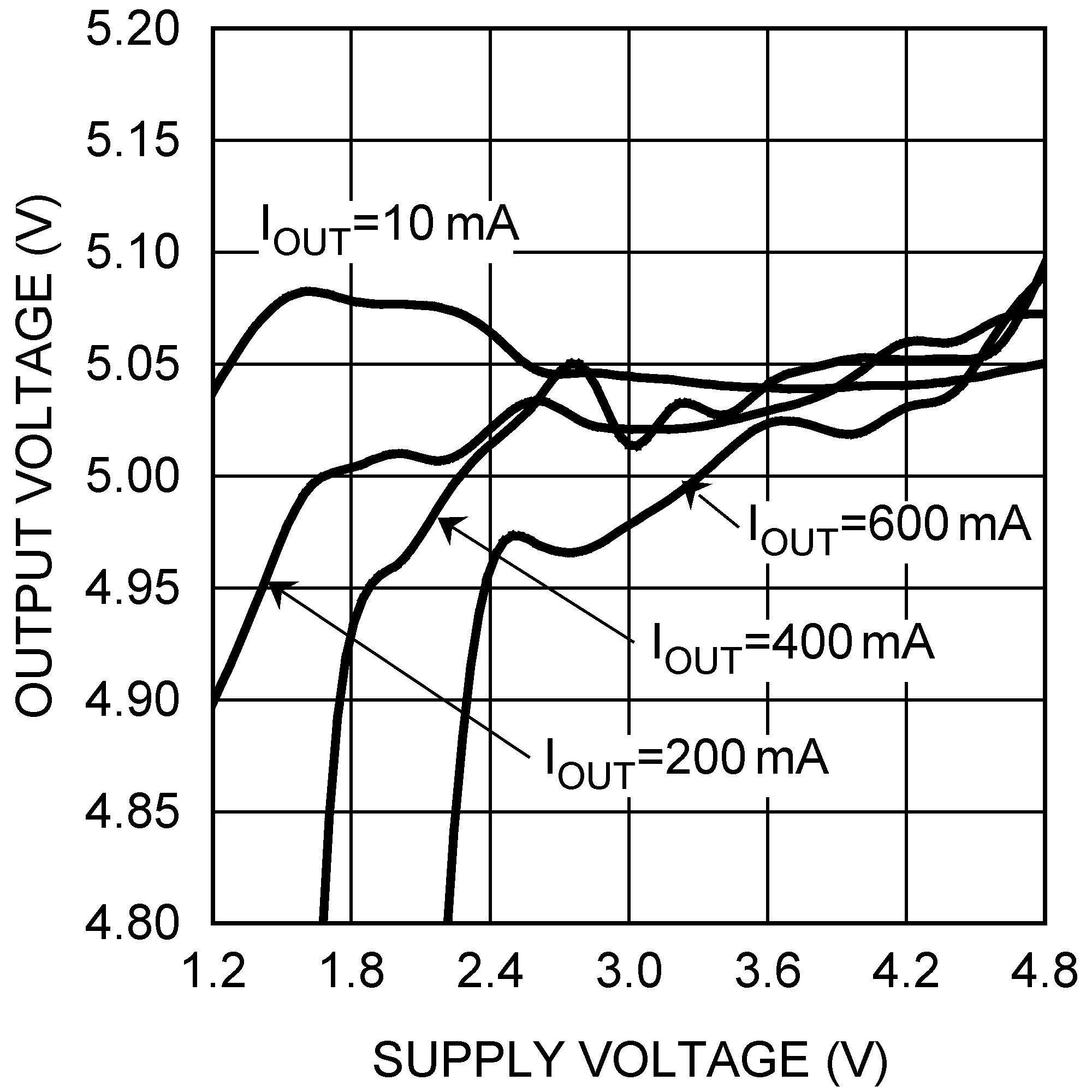
| VOUT = 5 V |
