SNVS457D February 2007 – October 2015 LM26400Y
PRODUCTION DATA.
- 1 Features
- 2 Applications
- 3 Description
- 4 Revision History
- 5 Pin Configuration and Functions
- 6 Specifications
- 7 Detailed Description
- 8 Application and Implementation
- 9 Power Supply Recommendations
- 10Layout
- 11Device and Documentation Support
- 12Mechanical, Packaging, and Orderable Information
封装选项
机械数据 (封装 | 引脚)
散热焊盘机械数据 (封装 | 引脚)
- PWP|16
订购信息
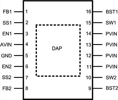
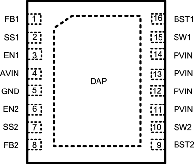
5 Pin Configuration and Functions
PWP Package
16-Pin HTSSOP With PowerPAD IC Package
Top View

NHQ Package
16-Pin WSON
Top View

Pin Functions
| PIN | TYPE | DESCRIPTION | |
|---|---|---|---|
| NAME | NO. | ||
| AVIN | 4 | PWR | Input supply for generating the internal bias used by the entire IC and for generating the internal bootstrap bias. Needs to be locally bypassed. |
| BST1 | 16 | O | Supply rail for the gate drive of Channel 1's NMOS switch. A bootstrap capacitor should be placed between the BST1 and SW1 pins. |
| BST2 | 9 | O | Supply rail for the gate drive of Channel 2's NMOS switch. A bootstrap capacitor should be placed between the BST2 and SW2 pins. |
| EN1 | 3 | I | Enable control input for Channel 1. Logic high enables operation. Do not allow this pin to float or be greater than VIN + 0.3 V. |
| EN2 | 6 | I | Enable control input for Channel 2. Logic high enables operation. Do not allow this pin to float or be greater than VIN + 0.3 V. |
| FB1 | 1 | I | Feedback pin of Channel 1. Connect FB1 to an external voltage divider to set the output voltage of Channel 1. |
| FB2 | 8 | I | Feedback pin of Channel 2. Connect FB2 to an external voltage divider to set the output voltage of Channel 2. |
| GND | 5 | PWR | Signal and Power ground pin. Kelvin connect the lower resistor of the feedback voltage divider to this pin for good load regulation. |
| PVIN | 11, 12, 13,14 | PWR | Input voltage of the power supply. Directly connected to the drain of the internal NMOS switch. Tie these pins together and connect to a local bypass capacitor. |
| SS1 | 2 | I | Soft start pin of Channel 1. Connect a capacitor between this pin and ground to program the start up speed. |
| SS2 | 7 | I | Soft start pin of Channel 2. Connect a capacitor between this pin and ground to program the start up speed. |
| SW2 | 10 | O | Switch node of Channel 2. Connects to the inductor, catch diode, and bootstrap capacitor. |
| SW1 | 15 | O | Switch node of Channel 1. Connects to the inductor, catch diode, and bootstrap capacitor. |
| Die Attach Pad | DAP | — | Must be connected to system ground for low thermal impedance and low grounding inductance. |