ZHCSI85A May 2018 – July 2019 LM26420-Q1
PRODUCTION DATA.
- 1 特性
- 2 应用
- 3 说明
- 4 修订历史记录
- 5 Pin Configuration and Functions
- 6 Specifications
- 7 Detailed Description
- 8 Application and Implementation
- 9 Power Supply Recommendations
- 10Layout
- 11器件和文档支持
- 12机械、封装和可订购信息
封装选项
机械数据 (封装 | 引脚)
散热焊盘机械数据 (封装 | 引脚)
订购信息
9 Power Supply Recommendations
The LM26420-Q1 is designed to operate from an input voltage supply range between 3 V and 5.5 V. This input supply must be well regulated and able to withstand maximum input current and maintain a stable voltage. The resistance of the input supply rail must be low enough that an input current transient does not cause a high enough drop at the LM26420-Q1 supply voltage that can cause a false UVLO fault triggering and system reset. If the input supply is located more than a few inches from the LM26420-Q1, additional bulk capacitance may be required in addition to the ceramic bypass capacitors. The amount of bulk capacitance is not critical, but a 47-μF or 100-μF electrolytic capacitor is a typical choice.
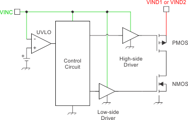
LM26420-Q1 contains a high side PMOS FET and a low side NMOS FET as shown in Figure 42. The source nodes of the high side PMOS FETs are connected to VIND1 and VIND2 respectively. VINC is the power source for the high and low side gate drivers. Ideally, VINC is connected to VIND1 and VIND2 by an RC filter as detailed in VINC Filtering Components . If VINC is allowed to be lower than VIND1 or VIND2, the high side PMOS FETs may be turned on regardless of the state of the respective gate drivers. Under this condition, shoot through will occur when the low side NMOS FET is turned on and permanent damage may result. When applying input voltage to VINC, VIND1 and VIND2, VINC must not be less than VIND1,2 – VTH to avoid shoot through and FET damage.
 Figure 42. VINC, VIND1 and VIND2 Connection