ZHCSI85A May 2018 – July 2019 LM26420-Q1
PRODUCTION DATA.
- 1 特性
- 2 应用
- 3 说明
- 4 修订历史记录
- 5 Pin Configuration and Functions
- 6 Specifications
- 7 Detailed Description
- 8 Application and Implementation
- 9 Power Supply Recommendations
- 10Layout
- 11器件和文档支持
- 12机械、封装和可订购信息
封装选项
机械数据 (封装 | 引脚)
散热焊盘机械数据 (封装 | 引脚)
订购信息
5 Pin Configuration and Functions
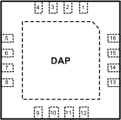
RUM Package
16-Pin WQFN
Top View

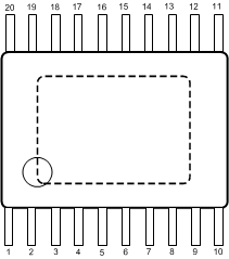
PWP Package
20-Pin HTSSOP
Top View

Pin Functions: 16-Pin WQFN
| PIN | TYPE | DESCRIPTION | |
|---|---|---|---|
| NUMBER | NAME | ||
| 1,2 | VIND1 | P | Power input supply for Buck 1. |
| 3 | SW1 | P | Output switch for Buck 1. Connect to the inductor. |
| 4 | PGND1 | G | Power ground pin for Buck 1. |
| 5 | FB1 | A | Feedback pin for Buck 1. Connect to external resistor divider to set output voltage. |
| 6 | PG1 | G | Power Good Indicator for Buck 1. Pin is connected through a resistor to an external supply (open drain output). |
| 7 | PG2 | G | Power Good Indicator for Buck 2. Pin is connected through a resistor to an external supply (open drain output). |
| 8 | FB2 | A | Feedback pin for Buck 2. Connect to external resistor divider to set output voltage. |
| 9 | PGND2 | G | Power ground pin for Buck 2. |
| 10 | SW2 | P | Output switch for Buck 2. Connect to the inductor. |
| 11, 12 | VIND2 | A | Power Input supply for Buck 2. |
| 13 | EN2 | A | Enable control input. Logic high enable operation for Buck 2. Do not allow this pin to float or be greater than VIN + 0.3 V. |
| 14 | AGND | G | Signal ground pin. Place the bottom resistor of the feedback network as close as possible to pin. |
| 15 | VINC | A | Input supply for control circuitry. |
| 16 | EN1 | A | Enable control input. Logic high enable operation for Buck 1. Do not allow this pin to float or be greater than VIN + 0.3 V. |
| DAP | Die Attach Pad | — | Connect to system ground for low thermal impedance and as a primary electrical GND connection. |
Pin Functions 20-Pin HTSSOP
| PIN | TYPE | DESCRIPTION | |
|---|---|---|---|
| NUMBER | NAME | ||
| 1 | VINC | A | Input supply for control circuitry. |
| 2 | EN1 | A | Enable control input. Logic high enable operation for Buck 1. Do not allow this pin to float or be greater than VIN + 0.3 V. |
| 3, 4 | VIND1 | A | Power Input supply for Buck 1. |
| 5 | SW1 | P | Output switch for Buck 1. Connect to the inductor. |
| 6,7 | PGND1 | G | Power ground pin for Buck 1. |
| 8 | FB1 | A | Feedback pin for Buck 1. Connect to external resistor divider to set output voltage. |
| 9 | PG1 | G | Power Good Indicator for Buck 1. Pin is connected through a resistor to an external supply (open drain output). |
| 10, 11, DAP | Die Attach Pad | — | Connect to system ground for low thermal impedance, but it cannot be used as a primary GND connection. |
| 12 | PG2 | G | Power Good Indicator for Buck 2. Pin is connected through a resistor to an external supply (open drain output). |
| 13 | FB2 | A | Feedback pin for Buck 2. Connect to external resistor divider to set output voltage. |
| 14, 15 | PGND2 | G | Power ground pin for Buck 2. |
| 16 | SW2 | P | Output switch for Buck 2. Connect to the inductor. |
| 17, 18 | VIND2 | A | Power Input supply for Buck 2. |
| 19 | EN2 | A | Enable control input. Logic high enable operation for Buck 2. Do not allow this pin to float or be greater than VIN + 0.3 V. |
| 20 | AGND | G | Signal ground pin. Place the bottom resistor of the feedback network as close as possible to pin. |