ZHCSD82C January 2015 – November 2017 LM26480-Q1
PRODUCTION DATA.
- 1 特性
- 2 应用
- 3 说明
- 4 修订历史记录
- 5 Device Comparison Tables
- 6 Pin Configuration and Functions
-
7 Specifications
- 7.1 Absolute Maximum Ratings
- 7.2 ESD Ratings
- 7.3 Recommended Operating Conditions: Bucks
- 7.4 Thermal Information
- 7.5 General Electrical Characteristics
- 7.6 Low Dropout Regulators, LDO1 and LDO2
- 7.7 Buck Converters SW1, SW2
- 7.8 I/O Electrical Characteristics
- 7.9 Power-On Reset Threshold/Function (POR)
- 7.10 Typical Characteristics — LDO
- 7.11 Typical Characteristics — Buck 2.8 V to 5.5 V
- 7.12 Typical Characteristics — Bucks 1 and 2
- 7.13 Typical Characteristics — Buck 3.6 V
-
8 Detailed Description
- 8.1 Overview
- 8.2 Functional Block Diagram
- 8.3
Feature Description
- 8.3.1
DC-DC Converters
- 8.3.1.1 Linear Low Dropout Regulators (LDOs)
- 8.3.1.2
SW1, SW2: Synchronous Step-Down Magnetic DC-DC Converters
- 8.3.1.2.1 Functional Description
- 8.3.1.2.2 Circuit Operation Description
- 8.3.1.2.3 PWM Operation
- 8.3.1.2.4 Internal Synchronous Rectification
- 8.3.1.2.5 Current Limiting
- 8.3.1.2.6 PFM Operation
- 8.3.1.2.7 SW1, SW2 Control
- 8.3.1.2.8 Shutdown Mode
- 8.3.1.2.9 Soft Start
- 8.3.1.2.10 Low Dropout Operation
- 8.3.1.2.11 Flexible Power-On Reset (Power Good with Delay)
- 8.3.1.2.12 Undervoltage Lockout
- 8.3.1
DC-DC Converters
- 8.4 Device Functional Modes
-
9 Application and Implementation
- 9.1 Application Information
- 9.2
Typical Application
- 9.2.1 Design Requirements
- 9.2.2 Detailed Design Procedure
- 9.2.3 Application Curves
- 10Power Supply Recommendations
- 11Layout
- 12器件和文档支持
- 13机械、封装和可订购信息
11 Layout
11.1 Layout Guidelines
PC board layout is an important part of DC-DC converter design. Poor board layout can disrupt the performance of a DC-DC converter and surrounding circuitry by contributing to EMI, ground bounce, and resistive voltage loss ii the traces. These can send erroneous signals to the DC-DC converter device, resulting in poor regulation or instability. Poor layout can also result in re-flow problems leading to poor solder joints, which can result in erratic or degraded performance.
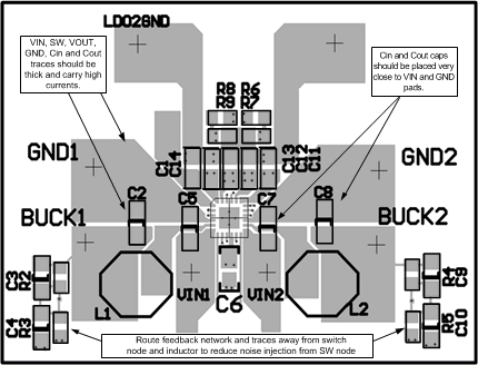
Good layout for the LM26480-Q1 bucks can be implemented by following a few simple design rules, as shown in Figure 34.
- Place the buck inductor and filter capacitors close together and make the trace short. The traces between these components carry relatively high switching currents and act as antennas. Following this rule reduces radiated noise. Place the capacitors and inductor close to the buck.
- Arrange the components so that the switching current loops curl in the same direction. During the first halt of each cycle, current flows from the input filter capacitor, through the buck and inductor to the output filter capacitor and back through ground, forming a current loop. In the second half of each cycle, current is pulled up from ground, through the buck by the inductor, to the output filter capacitor and then back through ground, forming a second current loop. Routing these loops so the current curls in the same direction prevents magnetic field reversal between the two half-cycles and reduces radiated noise.
- Connect the ground pins of the buck, and filter capacitors together using generous component-side copper fill as a pseudo-ground plane. Then connect this to the ground-plane (if one is used) with several vias. This reduces ground–plane noise by preventing the switching currents from circulating through the ground plane. It also reduces ground bounce at the buck by giving it a low-impedance ground connection.
- Use wide traces between the power components and for power connections to the DC-DC converter circuit. This reduces voltage errors caused by resistive losses across the traces
- ROUT noise sensitive traces, such as the voltage feedback path, away from noisy traces between the power components. The voltage feedback trace must remain close to the buck circuit and should be routed directly from FB to VOUT at the output capacitor and must be routed opposite to noise components. This reduces EMI radiated onto the DC-DC converter’s own voltage feedback trace.
In mobile phones, for example, a common practice is to place the DC-DC converter on one corner of the board, arrange the CMOS digital circuitry around it (because this also generates noise), and then place sensitive preamplifiers and IF stages on the diagonally opposing corner. Often, the sensitive circuitry is shielded with a metal pan and power to it is post-regulated to reduce conducted noise, using low-dropout linear regulators.
For more information on board layout techniques, refer to AN-1187 Leadless Leadframe Package (LLP) on TI's website. This application note also discusses package handling, solder stencil, and the assembly process.
11.2 Layout Example
 Figure 34. Board Layout Design Rules for the LM26480-Q1