ZHCSD82C January 2015 – November 2017 LM26480-Q1
PRODUCTION DATA.
- 1 特性
- 2 应用
- 3 说明
- 4 修订历史记录
- 5 Device Comparison Tables
- 6 Pin Configuration and Functions
-
7 Specifications
- 7.1 Absolute Maximum Ratings
- 7.2 ESD Ratings
- 7.3 Recommended Operating Conditions: Bucks
- 7.4 Thermal Information
- 7.5 General Electrical Characteristics
- 7.6 Low Dropout Regulators, LDO1 and LDO2
- 7.7 Buck Converters SW1, SW2
- 7.8 I/O Electrical Characteristics
- 7.9 Power-On Reset Threshold/Function (POR)
- 7.10 Typical Characteristics — LDO
- 7.11 Typical Characteristics — Buck 2.8 V to 5.5 V
- 7.12 Typical Characteristics — Bucks 1 and 2
- 7.13 Typical Characteristics — Buck 3.6 V
-
8 Detailed Description
- 8.1 Overview
- 8.2 Functional Block Diagram
- 8.3
Feature Description
- 8.3.1
DC-DC Converters
- 8.3.1.1 Linear Low Dropout Regulators (LDOs)
- 8.3.1.2
SW1, SW2: Synchronous Step-Down Magnetic DC-DC Converters
- 8.3.1.2.1 Functional Description
- 8.3.1.2.2 Circuit Operation Description
- 8.3.1.2.3 PWM Operation
- 8.3.1.2.4 Internal Synchronous Rectification
- 8.3.1.2.5 Current Limiting
- 8.3.1.2.6 PFM Operation
- 8.3.1.2.7 SW1, SW2 Control
- 8.3.1.2.8 Shutdown Mode
- 8.3.1.2.9 Soft Start
- 8.3.1.2.10 Low Dropout Operation
- 8.3.1.2.11 Flexible Power-On Reset (Power Good with Delay)
- 8.3.1.2.12 Undervoltage Lockout
- 8.3.1
DC-DC Converters
- 8.4 Device Functional Modes
-
9 Application and Implementation
- 9.1 Application Information
- 9.2
Typical Application
- 9.2.1 Design Requirements
- 9.2.2 Detailed Design Procedure
- 9.2.3 Application Curves
- 10Power Supply Recommendations
- 11Layout
- 12器件和文档支持
- 13机械、封装和可订购信息
7 Specifications
7.1 Absolute Maximum Ratings
over operating free-air temperature range (unless otherwise noted) (1)(2)| MIN | MAX | UNIT | ||
|---|---|---|---|---|
| VINLDO12, VIN1, AVDD, VIN2, VINLDO1, VINLDO2, ENSW1, FB1, FB2, ENSW2, ENLDO1, ENLDO2, SYNC, FBL1, FBL2 | −0.3 | 6 | V | |
| GND to GND SLUG | ±0.3 | |||
| Power dissipation, PD_MAX (TA = 85°C, TMAX = 125°C)(3) | 1.17 | W | ||
| Junction temperature, TJ-MAX | 150 | °C | ||
| Storage temperature, Tstg | −65 | 150 | °C | |
(1) Stresses beyond those listed under Absolute Maximum Ratings may cause permanent damage to the device. These are stress ratings only, which do not imply functional operation of the device at these or any other conditions beyond those indicated under Recommended Operating Conditions: Bucks. Exposure to absolute-maximum-rated conditions for extended periods may affect device reliability.
(2) All voltages are with respect to the potential at the GND pin.
(3) In applications where high power dissipation and/or poor package thermal resistance is present, the maximum ambient temperature may have to be derated. Maximum ambient temperature (TA-MAX) is dependent on the maximum operating junction temperature (TJ-MAX-OP = 125°C), the maximum power dissipation of the device in the application (PD-MAX), and the junction-to-ambient thermal resistance of the part/package in the application (RθJA), as given by the following equation: TA-MAX = TJ-MAX-OP − (RθJA × PD-MAX). See Application and Implementation.
7.2 ESD Ratings
| VALUE | UNIT | |||
|---|---|---|---|---|
| V(ESD) | Electrostatic discharge | Human-body model (HBM), per AEC Q100-002(1) | ±2000 | V |
| Charged-device model (CDM), per AEC Q100-011 | ±750 | |||
(1) AEC Q100-002 indicates that HBM stressing shall be in accordance with the ANSI/ESDA/JEDEC JS-001 specification.
7.3 Recommended Operating Conditions: Bucks
over operating free-air temperature range (unless otherwise noted)| MIN | NOM | MAX | UNIT | ||
|---|---|---|---|---|---|
| VIN | 2.8 | 5.5 | V | ||
| VEN | 0 | (VIN + 0.3 V) | |||
| Junction temperature, TJ | –40 | 125 | °C | ||
| Ambient temperature, TA(1) | –40 | 125 | °C | ||
(1) Junction-to-ambient thermal resistance is highly application and board-layout dependent. In applications where high maximum power dissipation exists, special care must be paid to thermal dissipation issues in board design.
7.4 Thermal Information
| THERMAL METRIC(1) | LM26480-Q1 | UNIT | |
|---|---|---|---|
| RTW (WQFN) | |||
| 24 PINS | |||
| RθJA | Junction-to-ambient thermal resistance | 32.7 | °C/W |
| RθJC(top) | Junction-to-case (top) thermal resistance | 31.2 | °C/W |
| RθJB | Junction-to-board thermal resistance | 11.2 | °C/W |
| ψJT | Junction-to-top characterization parameter | 0.2 | °C/W |
| ψJB | Junction-to-board characterization parameter | 11.2 | °C/W |
| RθJC(bot) | Junction-to-case (bottom) thermal resistance | 0.4 | °C/W |
(1) For more information about traditional and new thermal metrics, see the Semiconductor and IC Package Thermal Metrics application report.
7.5 General Electrical Characteristics
Unless otherwise noted, VIN = 3.6 V. Values and limits apply for TJ = 25°C.(1)(2)(3)| PARAMETER | TEST CONDITIONS | MIN | TYP | MAX | UNIT | |
|---|---|---|---|---|---|---|
| IQ | VINLDO12 shutdown current | VIN = 3.6 V | 0.5 | µA | ||
| VPOR | Power-on reset threshold | VDD falling edge(5) | 1.9 | V | ||
| TSD | Thermal shutdown threshold | See(4) | 160 | °C | ||
| TSDH | Thermal shutdown hysteresis | See(4) | 20 | |||
| UVLO | Undervoltage lockout | Rising | 2.9 | V | ||
| Failing | 2.7 | |||||
(1) Stresses beyond those listed under Absolute Maximum Ratings may cause permanent damage to the device. These are stress ratings only, which do not imply functional operation of the device at these or any other conditions beyond those indicated under Recommended Operating Conditions. Exposure to absolute-maximum-rated conditions for extended periods may affect device reliability.
(2) All voltages are with respect to the potential at the GND pin.
(3) Minimum (MIN) and maximum (MAX) limits are specified by design, test, or statistical analysis. Typical numbers represent the most likely norm.
(4) Specified by design. Not production tested.
(5) VPOR is voltage at which the EPROM resets. This is different from the UVLO on VINLDO12, which is the voltage at which the regulators shut off; and is also different from the nPOR function, which signals if the regulators are in a specified range.
7.6 Low Dropout Regulators, LDO1 and LDO2
Unless otherwise noted, VIN = 3.6 V, CIN = 1 µF, COUT = 0.47 µF, and values and limits apply for TJ = 25°C, unless otherwise specified. (1)(2)(3)(4)| PARAMETER | TEST CONDITIONS | MIN | TYP | MAX | UNIT | |
|---|---|---|---|---|---|---|
| VIN | Operational voltage range | VINLDO1 and VINLDO2 PMOS pins(5)
TJ = −40°C to 125°C |
1.74 | 5.5 | V | |
| VFB | FB voltage accuracy | TJ = −40°C to 125°C | –3% | 3% | ||
| ΔVOUT | Line regulation | VIN = (VOUT + 0.3 V) to 5 V(6)
Load current = 1 mA TJ = −40°C to 125°C |
0.15 | %/V | ||
| Load regulation | VIN = 3.6 V, TJ = −40°C to 125°C Load current = 1 mA to IMAX |
0.011 | %/mA | |||
| ISC | Short circuit current limit | LDO1-2, VOUT = 0 V | 500 | mA | ||
| VIN – VOUT | Dropout voltage | Load current = 50 mA(7)
|
25 | mV | ||
| Load current = 50 mA(7)
TJ = −40°C to 125°C |
200 | |||||
| PSRR | Power supply ripple rejection | F = 10 kHz, load current = IMAX | 45 | dB | ||
| eN | Supply output noise | 10 Hz < F < 100 kHz | 150 | µVRMS | ||
| IQ | Quiescent current on | IOUT = 0 mA | 40 | µA | ||
| IOUT = 0 mA, −40°C ≤ TJ ≤ 125°C | 150 | |||||
| Quiescent current on | IOUT = 300 mA | 60 | ||||
| IOUT = 300 mA, −40°C ≤ TJ ≤ 125°C | 200 | |||||
| Quiescent current off | EN is de-asserted | 0.03 | 1 | µA | ||
| TON | Turnon time | Start-up from shutdown | 300 | µsec | ||
| COUT | Output capacitor | Capacitance for stability 0°C ≤ TJ ≤ 125°C | 0.47 | µF | ||
| −40°C ≤ TJ ≤ 125°C | 0.33 | |||||
| −40°C ≤ TJ ≤ 125°C | 0.68 | 1 | ||||
| Equivalent series resistance (ESR) TJ = −40°C to 125°C |
5 | 500 | mΩ | |||
(1) All voltages are with respect to the potential at the GND pin.
(2) Minimum (MIN) and maximum (MAX) limits are specified by design, test, or statistical analysis. Typical (TYP) numbers represent the most likely norm.
(3) CIN, COUT: Low-ESR Surface-Mount Ceramic Capacitors (MLCCs) used in setting electrical characteristics.
(4) The device maintains a stable, regulated output voltage without a load.
(5) Pins 24, 19 can operate from VIN min of 1.74 V to a VIN max of 5.5 V. This rating is only for the series pass PMOS power FET. It allows the system design to use a lower voltage rating if the input voltage comes from a buck output.
(6) VIN minimum for line regulation values is 1.8 V.
(7) Dropout voltage is the voltage difference between the input and the output at which the output voltage drops to 100 mV below its nominal value.
7.7 Buck Converters SW1, SW2
Unless otherwise noted, VIN = 3.6 V, CIN = 10 µF, COUT = 10 µF, LOUT = 2.2 µH, and limits apply for TJ = 25°C, unless otherwise specified.(1) (2)(3)(4)| PARAMETER | TEST CONDITIONS | MIN | TYP | MAX | UNIT | |
|---|---|---|---|---|---|---|
| VFB(5) | Feedback voltage | −3% | 3% | |||
| VOUT | Line regulation | 2.8 V < VIN < 5.5 V IOUT = 10 mA |
0.089 | %/V | ||
| Load regulation | 100 mA < IOUT < IMAX | 0.0013 | %/mA | |||
| Eff | Efficiency | Load current = 250 mA | 96% | |||
| ISHDN | Shutdown supply current | EN is de-asserted | 0.01 | 1 | µA | |
| ƒOSC | Internal oscillator frequency | Default oscillator frequency = 2 MHz | 1.6 | 2 | 2.4 | MHz |
| Default oscillator frequency = 2.1 MHz | 2.1 | 2.5 | ||||
| Default oscillator frequency = 2.1 MHz TJ = −40°C to 125°C |
1.7 | |||||
| IPEAK | Buck1 peak switching current limit | 2 | 2.4 | A | ||
| Buck2 peak switching current limit | 2 | 2.4 | ||||
| IQ | Quiescent current on(6) | No load PFM mode | 33 | µA | ||
| No load PWM mode (forced PWM) | 2 | mA | ||||
| RDSON (P) | Pin-pin resistance PFET | 200 | 400 | mΩ | ||
| RDSON (N) | Pin-pin resistance NFET | 180 | 400 | |||
| TON | Turnon time | Start-up from shutdown | 500 | µsec | ||
| CIN | Input capacitor | Capacitance for stability | 10 | µF | ||
| COUT | Output capacitor | Capacitance for stability | 10 | |||
(1) All voltages are with respect to the potential at the GND pin.
(2) Minimum (MIN) and maximum (MAX) limits are specified by design, test, or statistical analysis. Typical (TYP) numbers represent the most likely norm.
(3) CIN, COUT: Low-ESR Surface-Mount Ceramic Capacitors (MLCCs) used in setting electrical characteristics.
(4) The device maintains a stable, regulated output voltage without a load.
(5) VIN ≥ VOUT + RDSON(P) (IOUT + 1/2 IRIPPLE). If these conditions are not met, voltage regulation will degrade as load increases.
(6) Quiescent current is defined here as the difference in current between the input voltage source and the load at VOUT.
7.8 I/O Electrical Characteristics
Limits apply over the entire junction temperature range for operation, TJ = −40°C to +125°C.| PARAMETER | TEST CONDITIONS | MIN | TYP | MAX | UNIT | |
|---|---|---|---|---|---|---|
| VIL | Input low level | 0.4 | V | |||
| VIH | Input high level | 0.7 × VDD | ||||
7.9 Power-On Reset Threshold/Function (POR)
| PARAMETER | TEST CONDITIONS | MIN | TYP | MAX | UNIT | |
|---|---|---|---|---|---|---|
| nPOR | nPOR = Power-on reset for Buck1 and Buck2 | Default = 60 ms | 60 | ms | ||
| Default = 130 µs | 130 | µs | ||||
| nPOR Threshold | Percentage of target voltage Buck1 or Buck2 | VBUCK1 AND VBUCK2 rising | 92% | |||
| VBUCK1 OR VBUCK2 falling | 82% | |||||
| VOL | Output level low | Load = IOL = 500 µA | 0.23 | 0.5 | V | |
7.10 Typical Characteristics — LDO
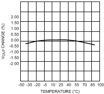
| VIN = 3.6 V | VOUT = 2.5 V | Load = 100 mA |
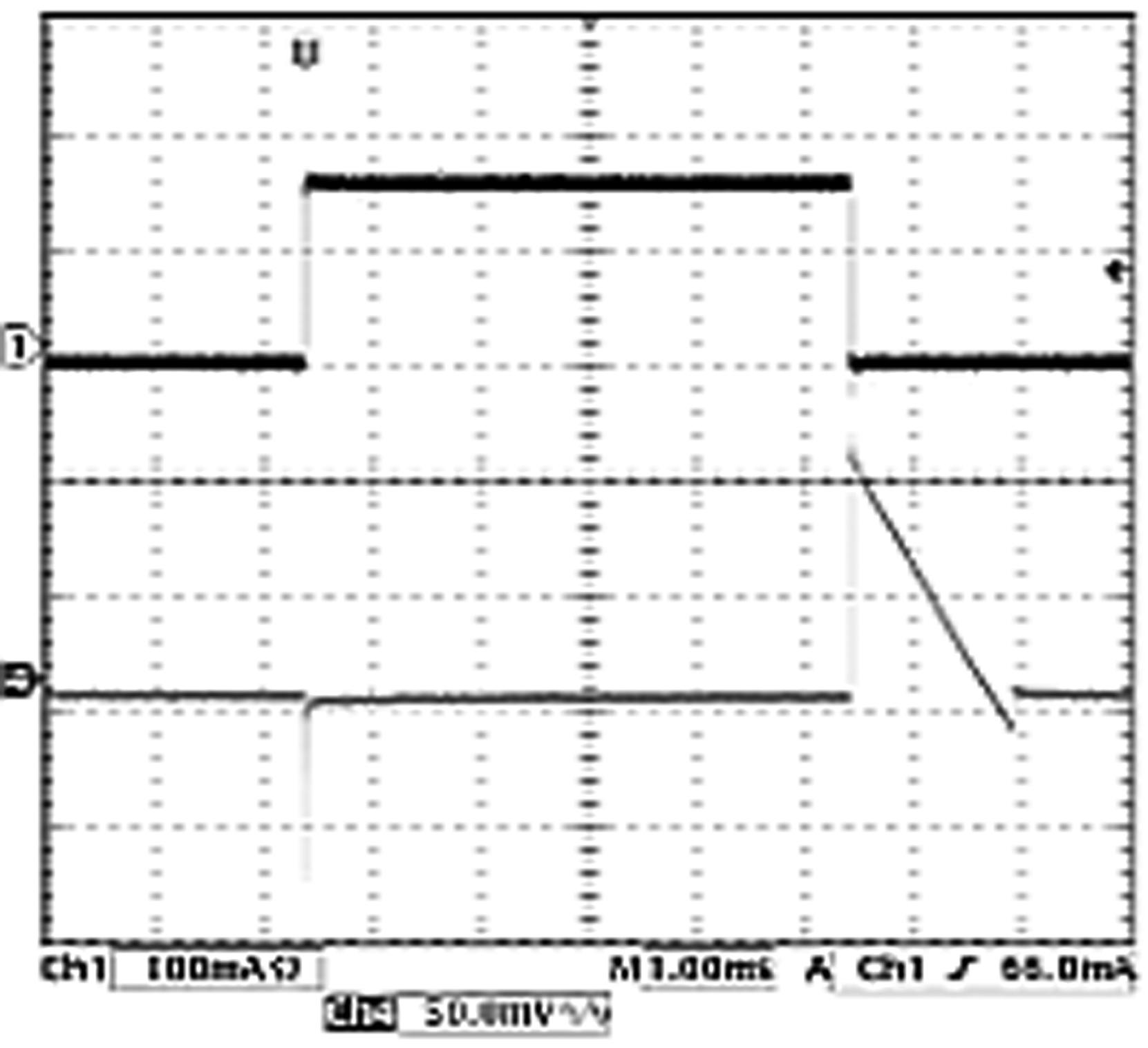
| VIN = 3.6 V | VOUT = 2.5 V | Load = 0 to 150 mA |
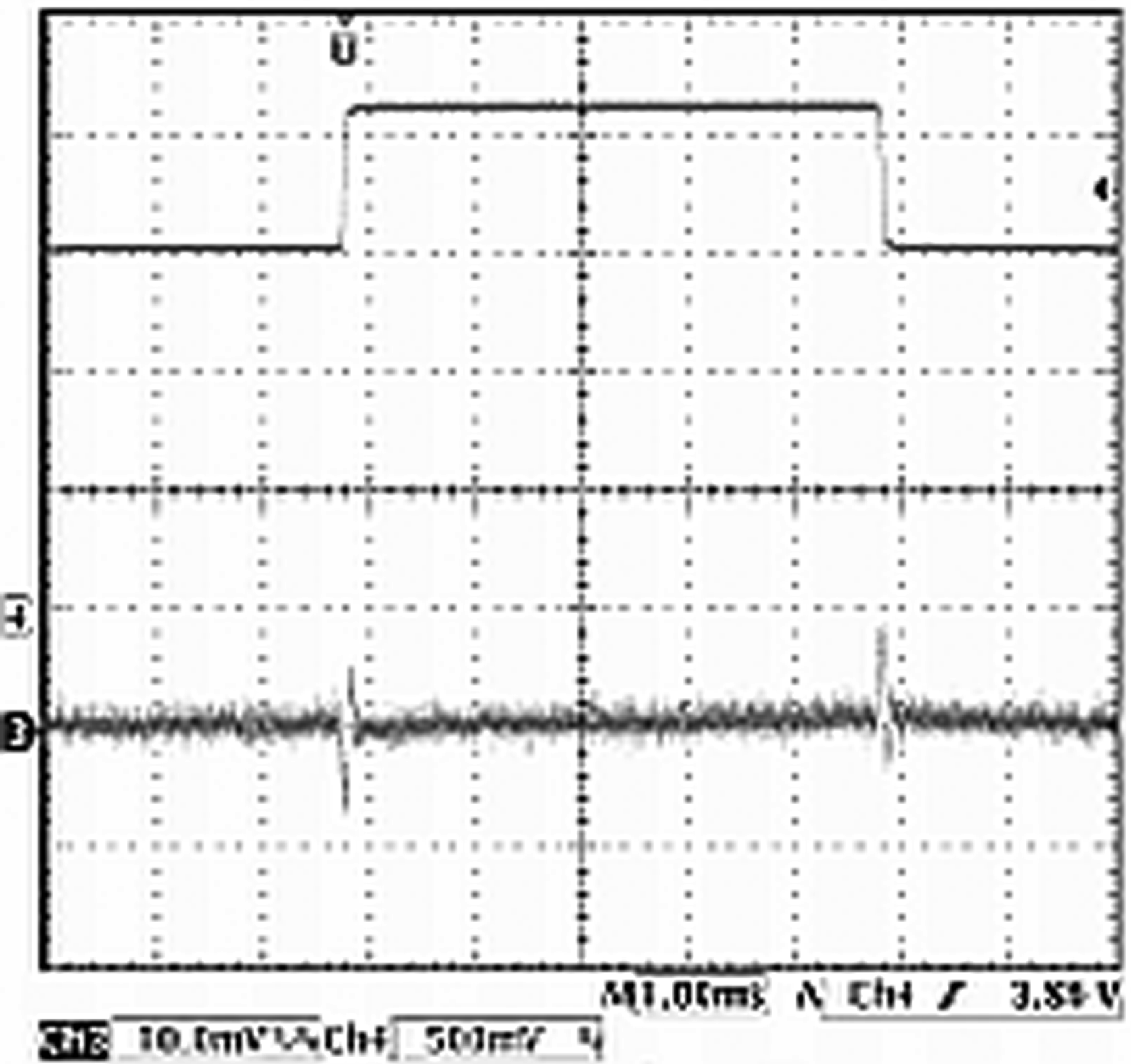
| VIN = 3.6 to 4.2 V | VOUT = 2.5 V | Load = 100 mA |
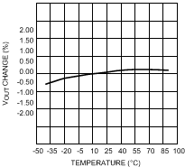
| VIN = 3.6 V | VOUT = 1.8 V | Load = 100 mA |
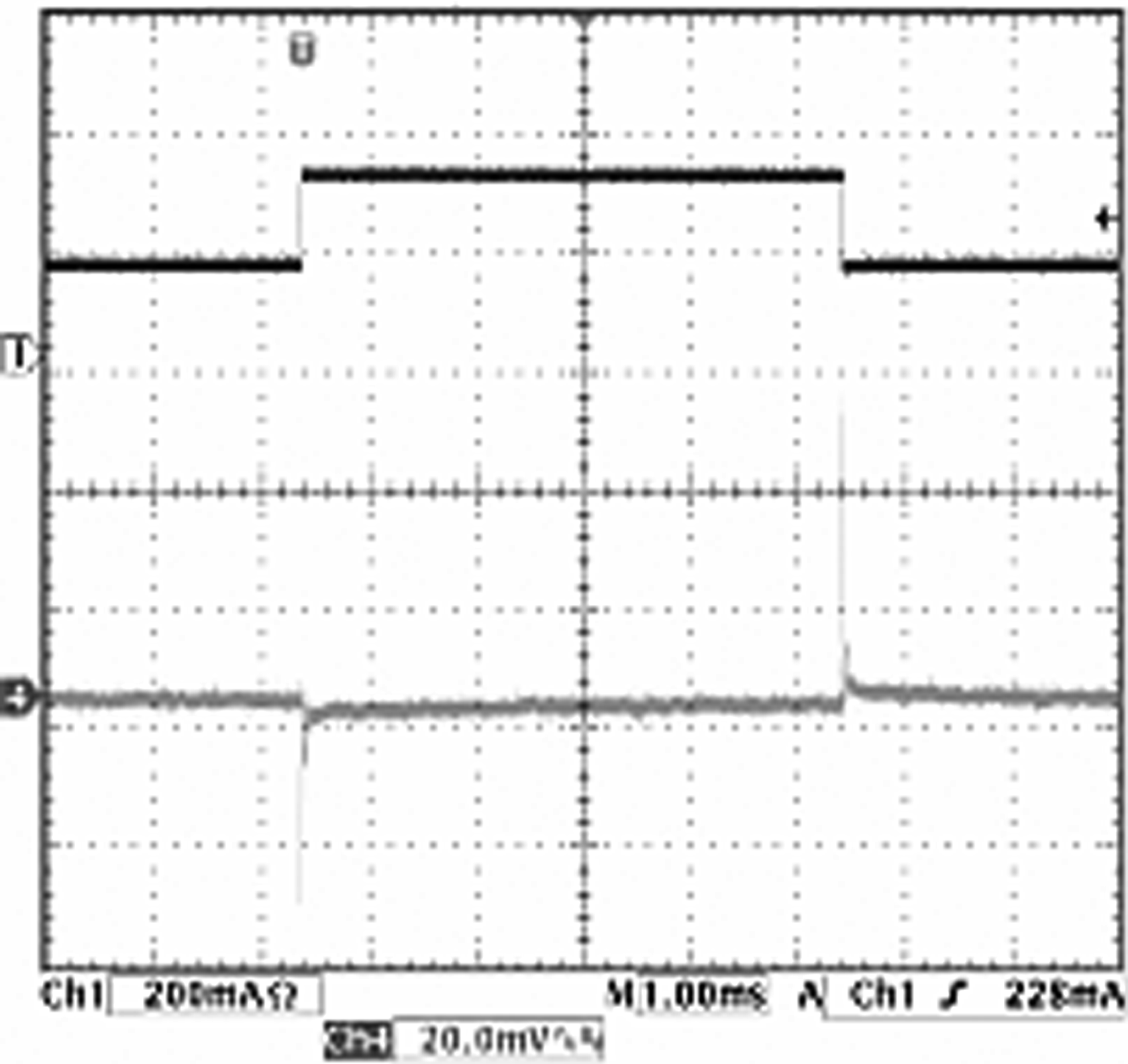
| VIN = 3.6 V | VOUT = 2.5 V | Load = 150 to 300 mA |
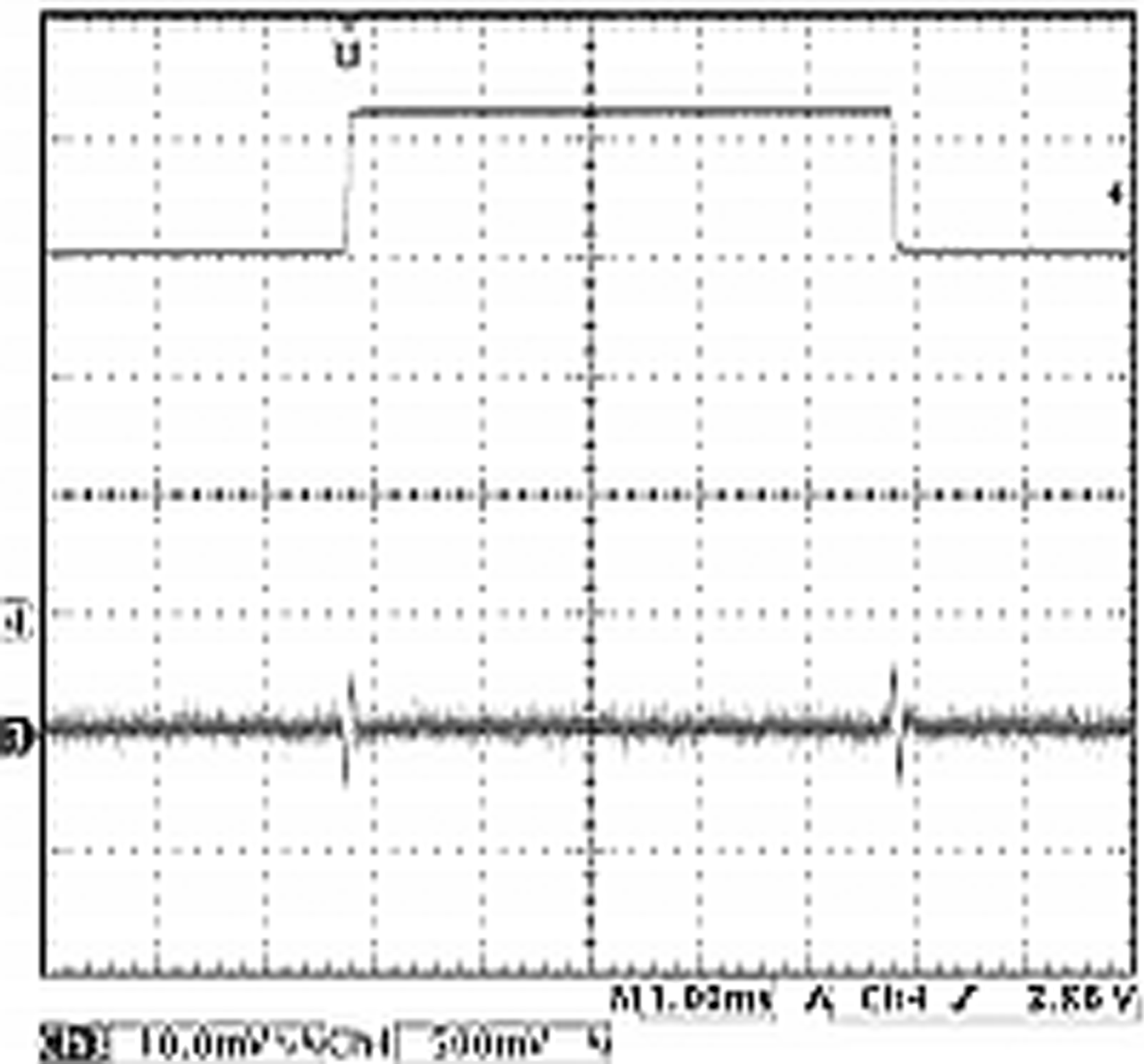
| VIN = 3.6 to 4.2 V | VOUT = 1.8 V | Load = 150 mA |
7.11 Typical Characteristics — Buck 2.8 V to 5.5 V
VIN = 2.8 V to 5.5 V, TA = 25°C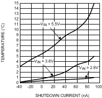
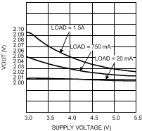
| VOUT = 2 V |
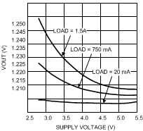
| VOUT = 1.2 V |
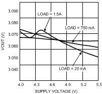
| VOUT = 3 V |
7.12 Typical Characteristics — Bucks 1 and 2
Output current transitions from PFM mode to PWM mode for Buck 1.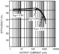
| VOUT = 1.2 V | L = 2.2 µH |
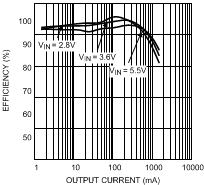
| VOUT = 2 V | L = 2.2 µH |
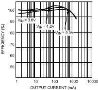
| VOUT = 3 V | L = 2.2 µH |

| VOUT = 3.5 V | L = 2.2 µH |
7.13 Typical Characteristics — Buck 3.6 V
VIN= 3.6 V, TA = 25°C, VOUT = 1.2 V unless otherwise noted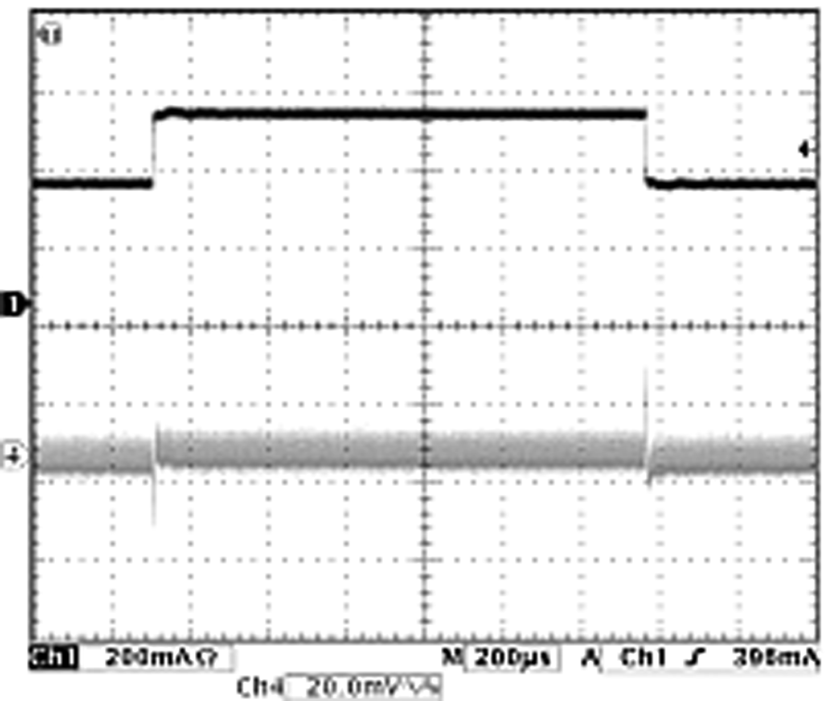
| VOUT = 1.2 V (PWM Mode) | ||
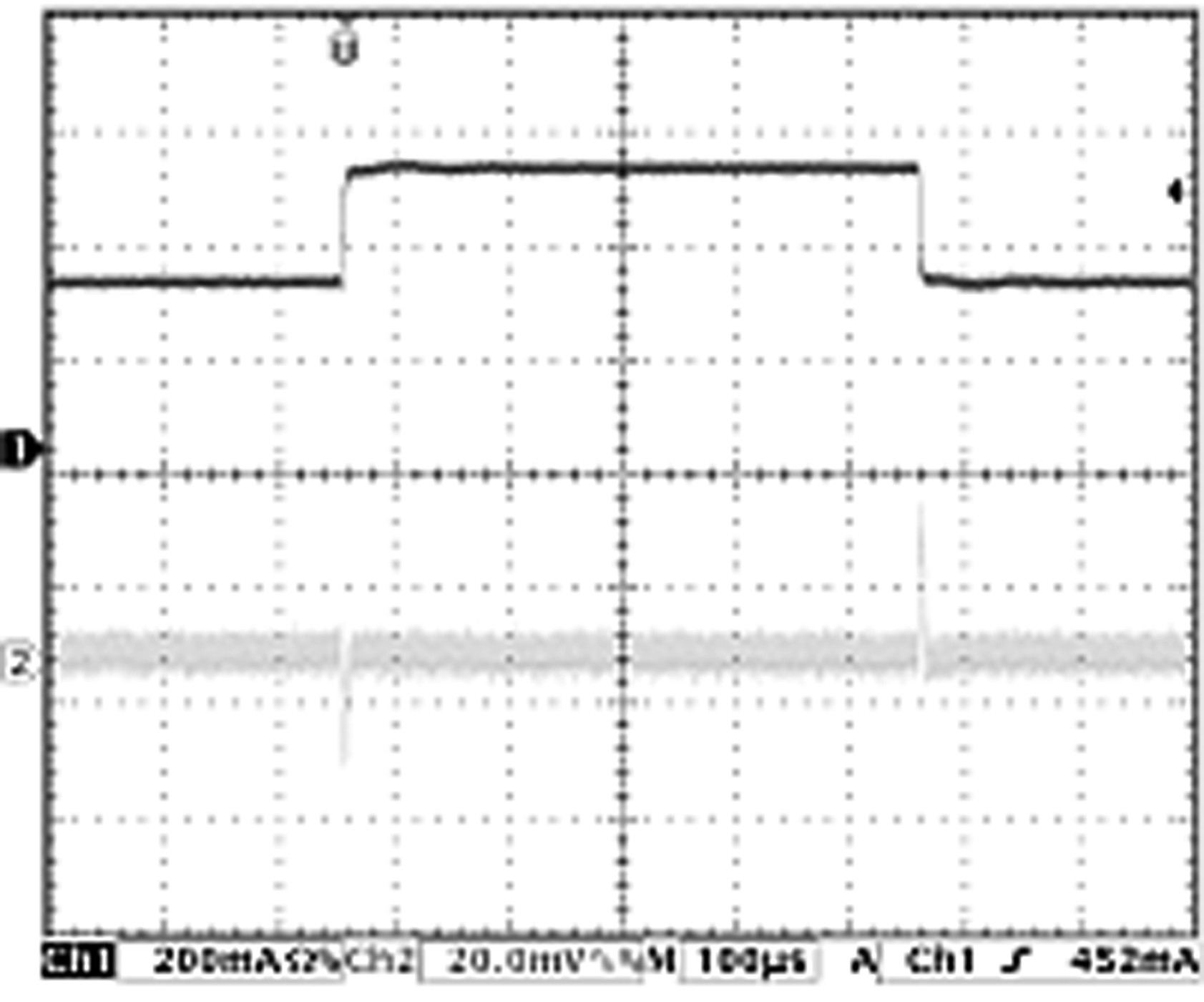
| VIN = 3.6 to 4.2 V | VOUT = 1.2 V | Load = 250 mA |
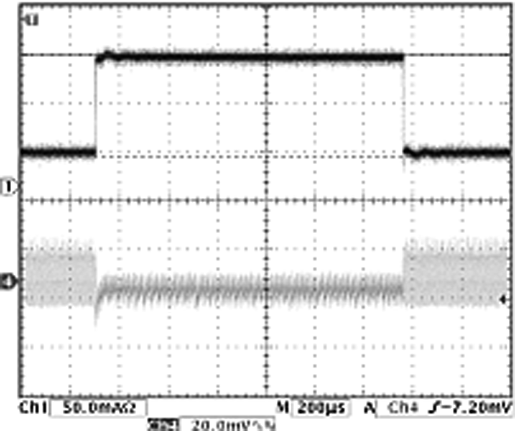
| VOUT = 1.2 V (PWM To PFM) | ||
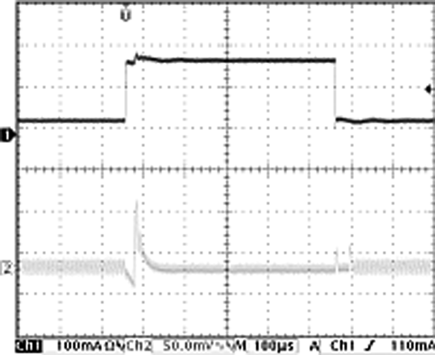
| VIN = 3 to 3.6 V | VOUT = 3 V | Load = 250 mA |