ZHCSD82C January 2015 – November 2017 LM26480-Q1
PRODUCTION DATA.
- 1 特性
- 2 应用
- 3 说明
- 4 修订历史记录
- 5 Device Comparison Tables
- 6 Pin Configuration and Functions
-
7 Specifications
- 7.1 Absolute Maximum Ratings
- 7.2 ESD Ratings
- 7.3 Recommended Operating Conditions: Bucks
- 7.4 Thermal Information
- 7.5 General Electrical Characteristics
- 7.6 Low Dropout Regulators, LDO1 and LDO2
- 7.7 Buck Converters SW1, SW2
- 7.8 I/O Electrical Characteristics
- 7.9 Power-On Reset Threshold/Function (POR)
- 7.10 Typical Characteristics — LDO
- 7.11 Typical Characteristics — Buck 2.8 V to 5.5 V
- 7.12 Typical Characteristics — Bucks 1 and 2
- 7.13 Typical Characteristics — Buck 3.6 V
-
8 Detailed Description
- 8.1 Overview
- 8.2 Functional Block Diagram
- 8.3
Feature Description
- 8.3.1
DC-DC Converters
- 8.3.1.1 Linear Low Dropout Regulators (LDOs)
- 8.3.1.2
SW1, SW2: Synchronous Step-Down Magnetic DC-DC Converters
- 8.3.1.2.1 Functional Description
- 8.3.1.2.2 Circuit Operation Description
- 8.3.1.2.3 PWM Operation
- 8.3.1.2.4 Internal Synchronous Rectification
- 8.3.1.2.5 Current Limiting
- 8.3.1.2.6 PFM Operation
- 8.3.1.2.7 SW1, SW2 Control
- 8.3.1.2.8 Shutdown Mode
- 8.3.1.2.9 Soft Start
- 8.3.1.2.10 Low Dropout Operation
- 8.3.1.2.11 Flexible Power-On Reset (Power Good with Delay)
- 8.3.1.2.12 Undervoltage Lockout
- 8.3.1
DC-DC Converters
- 8.4 Device Functional Modes
-
9 Application and Implementation
- 9.1 Application Information
- 9.2
Typical Application
- 9.2.1 Design Requirements
- 9.2.2 Detailed Design Procedure
- 9.2.3 Application Curves
- 10Power Supply Recommendations
- 11Layout
- 12器件和文档支持
- 13机械、封装和可订购信息
8 Detailed Description
8.1 Overview
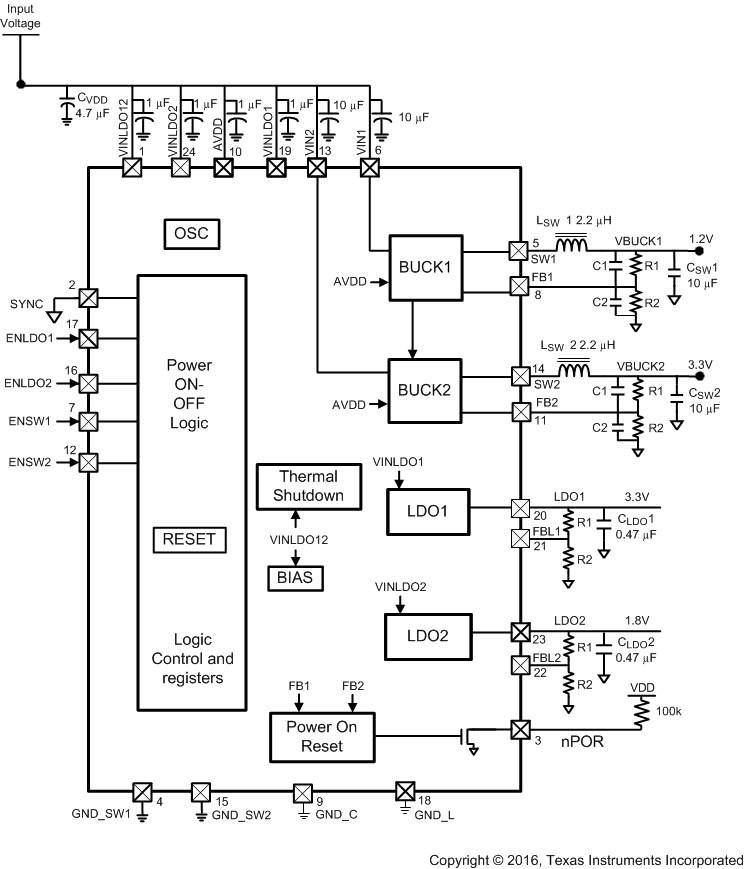
The LM26480-Q1 is a multi-functional power management unit (PMU), optimized for low-power digital applications. This device integrates two highly efficient 1.5-A step-down DC-DC converters and two 300-mA linear regulators.
8.2 Functional Block Diagram
8.3 Feature Description
8.3.1 DC-DC Converters
The LM26480-Q1 provides the DC-DC converters that supply the various power needs of the application by means of two linear low dropout regulators, LDO1 and LDO2, and two buck converters, SW1 and SW2. Table 3 lists the output characteristics of the various regulators.
Table 3. Supply Specification
| SUPPLY | LOAD | OUTPUT | |
|---|---|---|---|
| VOUT RANGE (V) | IMAX
MAXIMUM OUTPUT CURRENT (mA) |
||
| LDO1 | analog | 1 to 3.5 | 300 |
| LDO2 | analog | 1 to 3.5 | 300 |
| SW1 | digital | 0.8 to 2 | 1500 |
| SW2 | digital | 1 to 3.3 | 1500 |
8.3.1.1 Linear Low Dropout Regulators (LDOs)
LDO1 and LDO2 are identical linear regulators targeting analog loads characterized by low noise requirements. LDO1 and LDO2 are enabled through the ENLDO pin.
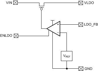 Figure 19. LDO Block Diagram
8.3.1.1.1 No-Load Stability
The LDOs remain stable and in regulation with no external load. This is an important consideration in some circuits, for example, CMOS RAM keep-alive applications.
8.3.1.2 SW1, SW2: Synchronous Step-Down Magnetic DC-DC Converters
8.3.1.2.1 Functional Description
The LM26480-Q1 incorporates two high-efficiency synchronous switching buck regulators, SW1 and SW2, that deliver a constant voltage from a single Li-Ion battery to the portable system processors. Using a voltage mode architecture with synchronous rectification, both bucks have the ability to deliver up to 1500 mA depending on the input voltage and output voltage (voltage headroom), and the inductor chosen (maximum current capability).
There are three modes of operation depending on the current required: PWM, PFM, and shutdown. PWM mode handles current loads of approximately 70 mA or higher, delivering voltage precision of ±3% with 90% efficiency or better. Lighter output current loads cause the device to automatically switch into PFM for reduced current consumption (IQ = 33 µA typical) and a longer battery life. The Standby operating mode turns off the device, offering the lowest current consumption. PWM or PFM mode is selected automatically or PWM mode can be forced through the setting of the buck control register.
Both SW1 and SW2 can operate up to a 100% duty cycle (PMOS switch always on) for low drop out control of the output voltage. In this way the output voltage will be controlled down to the lowest possible input voltage.
Additional features include soft-start, undervoltage lockout, current overload protection, and thermal overload protection.
The enable signal may be employed immediately after VIN is applied to the device. However, VIN must be stable for approximately 8 ms before enable single be asserted high to ensure internal bias, reference, and the flexible POR timing are stabilized. This initial delay is necessary only upon first time device power on.
8.3.1.2.2 Circuit Operation Description
A buck converter contains a control block, a switching PFET connected between input and output, a synchronous rectifying NFET connected between the output and ground (BCKGND pin) and a feedback path. During the first portion of each switching cycle, the control block turns on the internal PFET switch. This allows current to flow from the input through the inductor to the output filter capacitor and load. The inductor limits the current to a ramp with a slope of

by storing energy in a magnetic field. During the second portion of each cycle, the control block turns the PFET switch off, blocking current flow from the input, and then turns the NFET synchronous rectifier on. The inductor draws current from ground through the NFET to the output filter capacitor and load, which ramps the inductor current down with a slope of

The output filter stores charge when the inductor current is high, and releases it when low, smoothing the voltage across the load.
8.3.1.2.3 PWM Operation
During PWM operation the converter operates as a voltage-mode controller with input voltage feed forward. This allows the converter to achieve excellent load and line regulation. The DC gain of the power stage is proportional to the input voltage. To eliminate this dependence, feed forward voltage inversely proportional to the input voltage is introduced.
8.3.1.2.4 Internal Synchronous Rectification
While in PWM mode, the buck uses an internal NFET as a synchronous rectifier to reduce rectifier forward voltage drop and associated power loss. Synchronous rectification provides a significant improvement in efficiency whenever the output voltage is relatively low compared to the voltage drop across an ordinary rectifier diode.
8.3.1.2.5 Current Limiting
A current limit feature allows the converter to protect itself and external components during overload conditions. PWM mode implements current limiting using an internal comparator that trips at 2 A for both bucks (typical). If the output is shorted to ground the device enters a timed current limit mode where the NFET is turned on for a longer duration until the inductor current falls below a low threshold, ensuring inductor current has more time to decay, thereby preventing runaway.
8.3.1.2.6 PFM Operation
At very light loads, the converter enters PFM mode and operates with reduced switching frequency and supply current to maintain high efficiency.
The part will automatically transition into PFM mode when either of two conditions occurs for a duration of 32 or more clock cycles:
- The inductor current becomes discontinuous, or
- The peak PMOS switch current drops below the IMODE level.

During PFM operation, the converter positions the output voltage slightly higher than the nominal output voltage during PWM operation, allowing additional headroom for voltage drop during a load transient from light to heavy load. The PFM comparators sense the output voltage via the feedback pin and control the switching of the output FETs such that the output voltage ramps between 0.8% and 1.6% (typical) above the nominal PWM output voltage. If the output voltage is below the ‘high’ PFM comparator threshold, the PMOS power switch is turned on. It remains on until the output voltage exceeds the high PFM threshold or the peak current exceeds the IPFM level set for PFM mode. The typical peak current in PFM mode is:

Once the PMOS power switch is turned off, the NMOS power switch is turned on until the inductor current ramps to zero. When the NMOS zero-current condition is detected, the NMOS power switch is turned off. If the output voltage is below the ‘high’ PFM comparator threshold (see Figure 20), the PMOS switch is again turned on and the cycle is repeated until the output reaches the desired level. Once the output reaches the ‘high’ PFM threshold, the NMOS switch is turned on briefly to ramp the inductor current to zero and then both output switches are turned off and the part enters an extremely low power mode. Quiescent supply current during this ‘sleep’ mode is less than 30 µA, which allows the part to achieve high efficiencies under extremely light load conditions. When the output drops below the low PFM threshold, the cycle repeats to restore the output voltage to approximately 1.6% above the nominal PWM output voltage.
If the load current should increase during PFM mode (see Figure 20) causing the output voltage to fall below the ‘low2’ PFM threshold, the part will automatically transition into fixed-frequency PWM mode.
8.3.1.2.7 SW1, SW2 Control
SW1 and SW2 are enabled/disabled through the external enable pins.
The Modulation mode PWM/PFM is by default automatic and depends on the load (see Functional Description). The modulation mode can be factory trimmed, forcing the buck to operate in PWM mode regardless of the load condition.
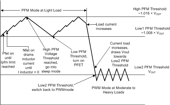 Figure 20. PWM/PFM Modulation
8.3.1.2.8 Shutdown Mode
During shutdown the PFET switch, reference, control and bias circuitry of the converters are turned off. The NFET switch will be on in shutdown to discharge the output. When the converter is enabled, soft start is activated. Disabling the converter during the system power up and undervoltage conditions is recommended when the supply is less than 2.8 V.
8.3.1.2.9 Soft Start
The soft-start feature allows the power converter to gradually reach the initial steady state operating point, thus reducing start-up stresses and surges. The two LM26480-Q1 buck converters have a soft-start circuit that limits in-rush current during start-up. During start-up the switch current limit is increased in steps. Soft start is activated only if EN goes from logic low to logic high after VIN reaches 2.8 V. Soft start is implemented by increasing switch current limit in steps of 250 mA, 500 mA, 950 mA, and 2 A for both bucks (typical switch current limit). The start-up time thereby depends on the output capacitor and load current demanded at start-up.
8.3.1.2.10 Low Dropout Operation
The LM26480-Q1 can operate at 100% duty cycle (no switching; PMOS switch completely on) for low dropout support of the output voltage. In this way the output voltage will be controlled down to the lowest possible input voltage. When the device operates near 100% duty cycle, output voltage ripple is approximately 25 mV. The minimum input voltage needed to support the output voltage is
where
- ILOAD = Load current
- RDSON, PFET = Drain to source resistance of PFET switch in the triode region
- RINDUCTOR = Inductor resistance
8.3.1.2.11 Flexible Power-On Reset (Power Good with Delay)
The LM26480-Q1 is equipped with an internal Power-On-Reset (POR) circuit which monitors the output voltage levels on bucks 1 and 2. The nPOR is an open drain logic output which is logic LOW when either of the buck outputs are below 92% of the rising value, or when one or both outputs fall below 82% of the desired value. The time delay between output voltage level and nPOR is enabled is (130 µs, 60 ms, 100 ms, 200 ms), 60 ms by default. For any other delay option, other than the default, please consult a Texas Instruments Sales Representative. The system designer can choose the external pull-up resistor (value such as 100 kΩ) for the nPOR pin.
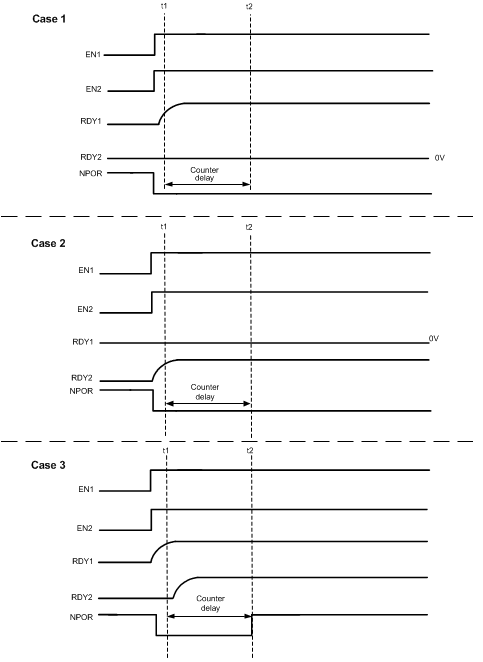 Figure 21. nPOR with Counter Delay
Figure 21 shows the simplest application of the POR where both switcher enables are tied together. In Case 1, EN1 causes nPOR to transition LOW and triggers the nPOR delay counter. If the power supply for Buck2 does not come on within that period, nPOR will stay LOW, indicating a power fail mode. Case 2 indicates the vice versa scenario if Buck1 supply did not come on. In both cases the nPOR remains LOW. Case 3 shows a typical application of the POR, where both switcher enables are tied together. Even if RDY1 ramps up slightly faster than RDY2 (or vice versa), the nPOR signal will trigger a programmable delay before going HIGH, as explained below.
 Figure 22. Faults Occurring in Counter Delay after Start-Up
Figure 22 details the Power Good with delay with respect to the enable signals EN1, and EN2. The RDY1, RDY2 are internal signals derived from the output of two comparators. Each comparator has been trimmed as follows:
Table 4. Comparator Trim
| COMPARATOR LEVEL | BUCK SUPPLY LEVEL |
|---|---|
| HIGH | Greater than 92% |
| LOW | Less than 82% |
The circuits for EN1 and RDY1 are symmetrical to EN2 and RDY2, so each reference to EN1 and RDY1 will also work for EN2 and RDY2 and vice versa.
If EN1 and RDY1 signals are High at time t1, then the RDY1 signal rising edge triggers the programmable delay counter (130 μs, 60 ms, 100 ms, 200 ms). This delay forces nPOR LOW between time interval t1 and t2. NPOR is then pulled high after the programmable delay is completed. Now if EN2 and RDY2 are initiated during this interval the nPOR signal ignores this event.
If either RDY1or RDY2 were to go LOW at t3 then the programmable delay is triggered again.
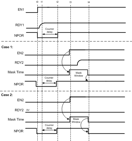 Figure 23. nPOR Mask Window
In Case 1 (Figure 23), we see that case where EN2 and RDY2 are initiated after triggered programmable delay. To prevent the nPOR being asserted again, a masked window (5 ms) counter delay is triggered off the EN2 rising edge. NPOR is still held HIGH for the duration of the mask, whereupon the nPOR status afterwards will depend on the status of both RDY1 and RDY2 lines.
In Case 2, we see the case where EN2 is initiated after the RDY1 triggered programmable delay, but RDY2 never goes HIGH (Buck2 never turns on). Normal operation operation of nPOR occurs wilth respect to EN1 and RDY1, and the nPOR signal is held HIGH for the duration of the mask window. We see that nPOR goes LOW after the masking window has timed out because it is now dependent on RDY1 and RDY2, where RDY2 is LOW.
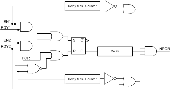 Figure 24. Design Implementation of the Flexible Power-On Reset
Design implementation of the flexible power-on reset. An internal power-on reset of the IC is used with EN1 and EN2 to produce a reset signal (LOW) to the delay timer nPOR. EN1 and RDY1 or EN2 and RDY2 are used to generate the set signal (HIGH) to the delay timer. S = R = 1 never occurs. The mask timers are triggered off EN1 and EN2 which are gated with RDY1, and RDY2 to generate outputs to the final AND gate to generate the nPOR.
8.3.1.2.12 Undervoltage Lockout
The LM26480-Q1 features an undervoltage lockout circuit. The function of this circuit is to continuously monitor the raw input supply voltage (VINLDO12) and automatically disable the four voltage regulators whenever this supply voltage is less than 2.8 VDC.
The circuit incorporates a bandgap based circuit that establishes the reference used to determine the 2.8 VDC trip point for a VIN OK – Not OK detector. This VIN OK signal is then used to gate the enable signals to the four regulators of the LM26480-Q1. When VINLDO12 is greater than 2.8 VDC the four enables control the four regulators; when VINLDO12 is less than 2.8 VDC the four regulators are disabled by the VIN detector being in the Not OK state. The circuit has built-in hysteresis to prevent undesired signal variations.
8.4 Device Functional Modes
There are two user-controlled modes of operations. The auto switch-over or auto-mode for the buck converters is that at high output current the regulator operates in the PWM mode. When the output draws relatively low current, in the neighborhood of 100 mA or less, the regulator automatically switches to the power-saving PFM mode. However, in the PFM mode, the switching frequency changes proportional to the amount of loading. In some applications it is not desirable to have variable switching frequencies. Hence, the forced PWM (FPWM) mode can be selected to retain a fixed nominal operating frequency to avoid interference or modulation issues in a system at the expense of slightly increased power consumption at light loads.