ZHCSD81N January 2008 – June 2017 LM26480
PRODUCTION DATA.
- 1 特性
- 2 应用
- 3 说明
- 4 修订历史记录
- 5 Device Options
- 6 Pin Configuration and Functions
-
7 Specifications
- 7.1 Absolute Maximum Ratings
- 7.2 ESD Ratings
- 7.3 Recommended Operating Conditions: Bucks
- 7.4 Thermal Information
- 7.5 General Electrical Characteristics
- 7.6 Low Dropout Regulators, LDO1 and LDO2
- 7.7 Buck Converters SW1, SW2
- 7.8 I/O Electrical Characteristics
- 7.9 Power On Reset Threshold/Function (POR)
- 7.10 Typical Characteristics — LDO
- 7.11 Typical Characteristics — Buck 2.8 V to 5.5 V
- 7.12 Typical Characteristics — Bucks 1 and 2
- 7.13 Typical Characteristics — Buck 3.6 V
-
8 Detailed Description
- 8.1 Overview
- 8.2 Functional Block Diagram
- 8.3
Feature Description
- 8.3.1
DC-DC Converters
- 8.3.1.1 Linear Low Dropout Regulators (LDOs)
- 8.3.1.2
SW1, SW2: Synchronous Step-Down Magnetic DC-DC Converters
- 8.3.1.2.1 Functional Description
- 8.3.1.2.2 Circuit Operation Description
- 8.3.1.2.3 Sync Function
- 8.3.1.2.4 PWM Operation
- 8.3.1.2.5 Internal Synchronous Rectification
- 8.3.1.2.6 Current Limiting
- 8.3.1.2.7 PFM Operation
- 8.3.1.2.8 SW1, SW2 Control
- 8.3.1.2.9 Shutdown Mode
- 8.3.1.2.10 Soft Start
- 8.3.1.2.11 Low Dropout Operation
- 8.3.1.2.12 Flexible Power-On Reset (Power Good with Delay)
- 8.3.1.2.13 Undervoltage Lockout
- 8.3.1
DC-DC Converters
- 8.4 Device Functional Modes
-
9 Application and Implementation
- 9.1 Application Information
- 9.2 Typical Application
- 10Power Supply Recommendations
- 11Layout
- 12器件和文档支持
- 13机械、封装和可订购信息
9 Application and Implementation
NOTE
Information in the following applications sections is not part of the TI component specification, and TI does not warrant its accuracy or completeness. TI’s customers are responsible for determining suitability of components for their purposes. Customers should validate and test their design implementation to confirm system functionality.
9.1 Application Information
9.1.1 External Component Selection
 Figure 25. LDO Block Diagram
Table 5. Buck External Component Selection
| TARGET VOUT (V) | IDEAL RESISTOR VALUES | COMMON R VALUES | ACTUAL VOUT w/ COM/R (V) | ACTUAL VOUT DELTA FROM TARGET (V) | FEEDBACK CAPACITORS | POWER RAIL |
|||
|---|---|---|---|---|---|---|---|---|---|
| R1 (KΩ) | R2 (KΩ) | R1 (KΩ) | R2 (KΩ) | C1 (pF) | C2 (pF) | ||||
| 0.8 | 120 | 200 | 121 | 200 | 0.803 | 0.002 | 15 | none | Buck1 |
| 0.9 | 160 | 200 | 162 | 200 | 0.905 | 0.005 | 15 | none | Only |
| 1 | 200 | 200 | 200 | 200 | 1 | 0 | 15 | none | ^ |
| 1.1 | 240 | 200 | 240 | 200 | 1.1 | 0 | 15 | none | | |
| 1.2 | 280 | 200 | 280 | 200 | 1.2 | 0 | 12 | none | | |
| 1.3 | 320 | 200 | 324 | 200 | 1.31 | 0.01 | 12 | none | Buck1 |
| 1.4 | 360 | 200 | 357 | 200 | 1.393 | -0.008 | 10 | none | And |
| 1.5 | 400 | 200 | 402 | 200 | 1.505 | 0.005 | 10 | none | Buck2 |
| 1.6 | 440 | 200 | 442 | 200 | 1.605 | 0.005 | 8.2 | none | | |
| 1.7 | 427 | 178 | 432 | 178 | 1.713 | 0.013 | 8.2 | none | | |
| 1.8 | 463 | 178 | 464 | 178 | 1.803 | 0.003 | 8.2 | none | | |
| 1.9 | 498 | 178 | 499 | 178 | 1.902 | 0.002 | 8.2 | none | | |
| 2 | 450 | 150 | 453 | 150 | 2.01 | 0.01 | 8.2 | none | > |
| 2.1 | 480 | 150 | 475 | 150 | 2.083 | -0.017 | 8.2 | none | ^ |
| 2.2 | 422 | 124 | 422 | 124 | 2.202 | 0.002 | 8.2 | none | | |
| 2.3 | 446 | 124 | 442 | 124 | 2.282 | -0.018 | 8.2 | none | | |
| 2.4 | 471 | 124 | 475 | 124 | 2.415 | 0.015 | 8.2 | none | | |
| 2.5 | 400 | 100 | 402 | 100 | 2.51 | 0.01 | 8.2 | none | | |
| 2.6 | 420 | 100 | 422 | 100 | 2.61 | 0.01 | 8.2 | none | | |
| 2.7 | 440 | 100 | 442 | 100 | 2.71 | 0.01 | 8.2 | 33 | Buck2 |
| 2.8 | 460 | 100 | 464 | 100 | 2.82 | 0.02 | 8.2 | 33 | Only |
| 2.9 | 480 | 100 | 475 | 100 | 2.875 | -0.025 | 8.2 | 33 | | |
| 3 | 500 | 100 | 499 | 100 | 2.995 | -0.005 | 6.8 | 33 | | |
| 3.1 | 520 | 100 | 523 | 100 | 3.115 | 0.015 | 6.8 | 33 | | |
| 3.2 | 540 | 100 | 536 | 100 | 3.18 | -0.02 | 6.8 | 33 | | |
| 3.3 | 560 | 100 | 562 | 100 | 3.31 | 0.01 | 6.8 | 33 | | |
The output voltages of the bucks of the LM26480 are established by the feedback resistor dividers R1 and R2 shown on the application circuit above. Equation 6 shows how to determine what value of V is:
where
- VFB is the voltage on the Buck FBx pin.
The Buck control loop will force the voltage on VFB to be 0.50 V ±3%.
Table 5 shows ideal resistor values to establish buck voltages from 0.8 V to 3.3 V along with common resistor values to establish these voltages. Common resistors do not always produce the target value, error is given in the delta column.
In addition to the resistor feedback, capacitor feedback C1 is always required, and depending on the output voltage capacitor C2 is also required.
| INDUCTOR | VALUE | UNIT | DESCRIPTION | NOTES |
|---|---|---|---|---|
| LSW1,2 | 2.2 | µH | SW1,2 inductor | DCR 70 mΩ |
9.1.2 Feedback Resistors for LDOs
See Figure 25.
Table 6. LDO External Component Selection
| TARGET VOUT (V) | IDEAL RESISTOR VALUES | COMMON R VALUES | ACTUAl VOUT W/Com/R (V) | ||
|---|---|---|---|---|---|
| R1 (KΩ) | R2 (KΩ) | R1 (KΩ) | R2 (KΩ) | ||
| 1 | 200 | 200 | 200 | 200 | 1 |
| 1.1 | 240 | 200 | 240 | 200 | 1.1 |
| 1.2 | 280 | 200 | 280 | 200 | 1.2 |
| 1.3 | 320 | 200 | 324 | 200 | 1.31 |
| 1.4 | 360 | 200 | 357 | 200 | 1.393 |
| 1.5 | 400 | 200 | 402 | 200 | 1.505 |
| 1.6 | 440 | 200 | 442 | 200 | 1.605 |
| 1.7 | 480 | 200 | 562 | 232 | 1.711 |
| 1.8 | 520 | 200 | 604 | 232 | 1.802 |
| 1.9 | 560 | 200 | 562 | 200 | 1.905 |
| 2 | 600 | 200 | 604 | 200 | 2.01 |
| 2.1 | 640 | 200 | 715 | 221 | 2.118 |
| 2.2 | 680 | 200 | 681 | 200 | 2.203 |
| 2.3 | 720 | 200 | 806 | 226 | 2.283 |
| 2.4 | 760 | 200 | 845 | 221 | 2.412 |
| 2.5 | 800 | 200 | 750 | 187 | 2.505 |
| 2.6 | 840 | 200 | 909 | 215 | 2.614 |
| 2.7 | 880 | 200 | 1100 | 249 | 2.709 |
| 2.8 | 920 | 200 | 1150 | 249 | 2.809 |
| 2.9 | 960 | 200 | 1210 | 255 | 2.873 |
| 3 | 1000 | 200 | 1000 | 200 | 3 |
| 3.1 | 1040 | 200 | 1000 | 191 | 3.118 |
| 3.2 | 1080 | 200 | 1000 | 187 | 3.174 |
| 3.3 | 1120 | 200 | 1210 | 215 | 3.314 |
| 3.4 | 1160 | 200 | 1210 | 210 | 3.381 |
| 3.5 | 1200 | 200 | 1210 | 200 | 3.525 |
The output voltages of the LDOs of the LM26480 are established by the feedback resistor dividers R1 and R2 shown on Figure 25 above. Equation 7 shows calculation for VOUT:
where
- VFB is the voltage on the LDOX_FB pin.
The LDO control loop will force the voltage on VFB to be 0.50 V ±3%. The above table shows ideal resistor values to establish LDO voltages from 1 V to 3.5 V along with common resistor values to establish these voltages. Common resistors do not always produce the target value, error is given in the final column.
To keep the power consumed by the feedback network low it is recommended that R2 be established as about 200 kΩ. Lesser values of R2 are okay at the users discretion.
9.2 Typical Application
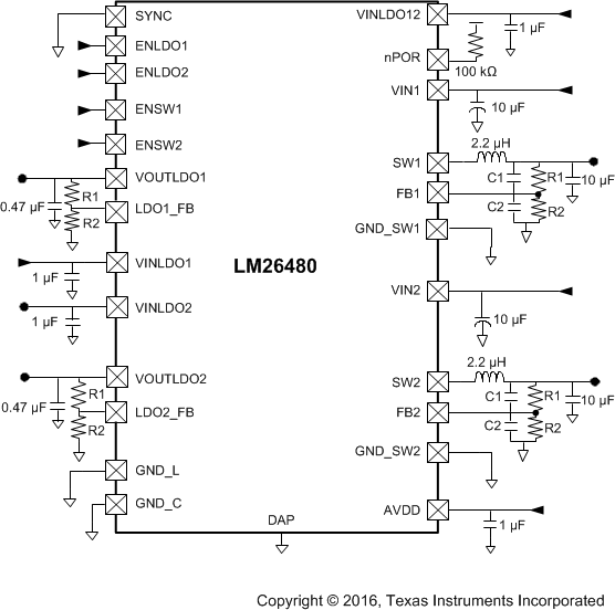 Figure 26. LM26480 Application Circuit
9.2.1 Design Requirements
9.2.1.1 High VIN- High Load Operation
Additional information is provided when the device is operated at extremes of VIN and regulator loads. These are described in terms of the junction temperature and buck output ripple management.
9.2.1.2 Junction Temperature
The maximum junction temperature TJ-MAX-OP of 125°C of the device package.
Equation 8 and Equation 9 demonstrate junction temperature determination, ambient temperature TA-MAX, and total chip power must be controlled to keep TJ below this maximum:
Total IC power dissipation PD-MAX is the sum of the individual power dissipation of the four regulators plus a minor amount for chip overhead. Chip overhead is bias, TSD, and LDO analog.
If VIN and ILOAD increase, the output ripple associated with the buck regulators also increases. This mainly occurs with VIN > 5.2 V and a load current greater than 1.2 A. To ensure operation in this area of operation, TI recommends that the system designer circumvents the output ripple issues by installing Schottky diodes on the bucks(s) that are expected to perform under these extreme conditions.
9.2.2 Detailed Design Procedure
9.2.2.1 Output Inductors and Capacitors for SW1 AND SW2
There are several design considerations related to the selection of output inductors and capacitors:
- Load transient response;
- Stability;
- Efficiency;
- Output ripple voltage; and
- Overcurrent ruggedness.
The LM26480 has been optimized for use with nominal values 2.2 µH and 10 µF. If other values are needed for the design, please contact Texas Instruments sales with any concerns.
9.2.2.1.1 Inductor Selection for SW1 and SW2
TI recommends a nominal inductor value of 2.2 µH. It is important to ensure the inductor core does not saturate during any foreseeable operational situation.
Care should be taken when reviewing the different saturation current ratings that are specified by different manufacturers. Saturation current ratings are typically specified at 25°C, so ratings at maximum ambient temperature of the application should be requested from the manufacturer.
There are two methods to choose the inductor saturation current rating:
Recommended method:
The best way to ensure the inductor does not saturate is to choose an inductor that has saturation current rating greater than the maximum LM26480 current limit of 2.4 A. In this case the device prevents inductor saturation.
Alternate method:
If the recommended approach cannot be used, care must be taken to ensure that the saturation current is greater than the peak inductor current:
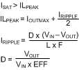
where
- ISAT: Inductor saturation current at operating temperature
- ILPEAK: Peak inductor current during worst case conditions
- IOUTMAX: Maximum average inductor current
- IRIPPLE: Peak-to-peak inductor current
- VOUT: Output voltage
- VIN: Input voltage
- L: Inductor value in Henries at IOUTMAX
- F: Switching frequency, Hertz
- D: Estimated duty factor
- EFF: Estimated power supply efficiency
ISAT may not be exceeded during any operation, including transients, start-up, high temperature, worst-case conditions, etc.
9.2.2.1.2 Suggested Inductors and Their Suppliers
| MODEL | MANUFACTURER | DIMENSIONS (mm) | DCR (max) (mΩ) | ISATURATION (A) (values approx.) |
|---|---|---|---|---|
| DO3314-222MX | Coilcraft | 3.3 × 3.3 × 1.4 | 200 | 1.8 |
| LPO3310-222MX | Coilcraft | 3.3 × 3.3 × 1 | 150 | 1.3 |
| ELL6PG2R2N | Panasonic | 6 × 6 × 2 | 37 | 2.2 |
| ELC6GN2R2N | Panasonic | 6 × 6 × 1.5 | 53 | 1.9 |
| CDRH2D14NP-2R2NC | Sumida | 3.2 × 3.2 × 1.5 | 94 | 1.5 |
9.2.2.2 Output Capacitor Selection for SW1 and SW2
TI recommends a ceramic output capacitor of 10 µF, 6.3 V with an ESR of less than 500 mΩ.
Output ripple can be estimated from the vector sum of the reactive (capacitor) voltage component and the real (ESR) voltage component of the output capacitor.

where
- VCOUT: Estimated reactive output ripple
- VROUT: Estimated real output ripple
- VPPOUT: Estimated peak-to-peak output ripple
The output capacitor needs to be mounted as close as possible to the output pin of the device. For better temperature performance, X7R or X5R types are recommended. DC bias characteristics of ceramic capacitors must be considered when selecting case sizes like 0805 and 0603.
DC bias characteristics vary from manufacturer to manufacturer and by case size. DC bias curves should be requested from them as part of the capacitor selection process. ESR is typically higher for smaller packages.
The output filter capacitor smooths out current flow from the inductor to the load, helps maintain a steady output voltage during transient load changes and reduces output voltage ripple. These capacitors must be selected with sufficient capacitance and sufficiently low ESR to perform these functions.
Note that the output voltage ripple is dependent on the inductor current ripple and the equivalent series resistance of the output capacitor (ESRCOUT). ESRCOUT is frequency dependent as well as temperature dependent. The RESR should be calculated with the applicable switching frequency and ambient temperature.
9.2.2.3 Input Capacitor Selection for SW1 and SW2
It is required to use a ceramic input capacitor of at least 4.7 μF and 6.3 V with an ESR of less than 500 mΩ.
The input power source supplies average current continuously. During the PFET switch on-time, however, the demanded di/dt is higher than can be typically supplied by the input power source. This delta is supplied by the input capacitor.
A simplified “worst case” assumption is that all of the PFET current is supplied by the input capacitor. This will result in conservative estimates of input ripple voltage and capacitor RMS current. Input ripple voltage is estimated in Equation 12:

where
- VPPIN: Estimated peak-to-peak input ripple voltage
- IOUT: Output current, Amps
- CIN: Input capacitor value, Farads
- ESRIN: Input capacitor ESR, Ohms
This capacitor is exposed to significant RMS current, so it is important to select a capacitor with an adequate RMS current rating. Capacitor RMS current estimated as follows:

where
- IRSCIN: Estimated input capacitor RMS current
Table 7. Suggested Capacitors and Their Suppliers
| MODEL | TYPE | VENDOR | VOLTAGE RATING (V) | CASE SIZE |
|---|---|---|---|---|
| 4.7 µF for CIN | ||||
| C2012X5R0J475K | Ceramic, X5R | TDK | 6.3 | 0805, (2012) |
| JMK212BJ475K | Ceramic, X5R | Taiyo-Yuden | 6.3 | 0805, (2012) |
| GRM21BR60J475K | Ceramic, X5R | Murata | 6.3 | 0805, (2012) |
| C1608X5R0J475K | Ceramic, X5R | TDK | 6.3 | 0603, (1608) |
| 10 µF for COUT | ||||
| GRM21BR60J106K | Ceramic, X5R | Murata | 6.3 | 0805, (2012) |
| JMK212BJ106K | Ceramic, X5R | Taiyo-Yuden | 6.3 | 0805, (2012) |
| C2012X5R0J106K | Ceramic, X5R | TDK | 6.3 | 0805, (2012) |
| C1608X5R0J106K | Ceramic, X5R | TDK | 6.3 | 0603, (1608) |
9.2.2.4 LDO Capacitor Selection
9.2.2.4.1 Input Capacitor
An input capacitor is required for stability. TI recommends that a 1-μF capacitor be connected between the LDO input pin and ground (this capacitance value may be increased without limit). This capacitor must be located a distance of not more than 1 cm from the input pin and returned to a clean analog ground. Any good quality ceramic, tantalum, or film capacitor may be used at the input.
CAUTION
Tantalum capacitors can suffer catastrophic failures due to surge currents when connected to a low impedance source of power (like a battery or a very large capacitor). If a tantalum capacitor is used at the input, it must be specified by the manufacturer to have a surge current rating sufficient for the application.
There are no requirements for the ESR on the input capacitor, but tolerance and temperature coefficient must be considered when selecting the capacitor to ensure the capacitance will remain approximately 1 μF over the entire operating temperature range.
9.2.2.4.2 Output Capacitor
The LDOs on the LM26480 are designed specifically to work with very small ceramic output capacitors. A 1-μF ceramic capacitor (temperature types Z5U, Y5V, or X7R) with ESR between 5 mΩ to 500 mΩ, are suitable in the application circuit. It is also possible to use tantalum or film capacitors at the device output COUT (or VOUT), but these are not as attractive for reasons of size and cost. The output capacitor must meet the requirement for the minimum value of capacitance and also have an ESR value that is within the range 5 mΩ to 500 mΩ for stability.
9.2.2.4.3 Capacitor Characteristics
The LDOs are designed to work with ceramic capacitors on the output to take advantage of the benefits they offer. For capacitance values in the range of 0.47 μF to 4.7 μF, ceramic capacitors are the smallest, least expensive and have the lowest ESR values, thus making them best for eliminating high frequency noise. The ESR of a typical 1-μF ceramic capacitor is in the range of 20 mΩ to 40 mΩ, which easily meets the ESR requirement for stability for the LDOs.
For both input and output capacitors, careful interpretation of the capacitor specification is required to ensure correct device operation. The capacitor value can change greatly, depending on the operating conditions and capacitor type.
In particular, the output capacitor selection should take account of all the capacitor parameters, to ensure that the specification is met within the application. The capacitance can vary with DC bias conditions as well as temperature and frequency of operation. Capacitor values will also show some decrease over time due to aging. The capacitor parameters are also dependent on the particular case size, with smaller sizes giving poorer performance figures in general. As an example, Figure 27 shows a typical graph comparing different capacitor case sizes in a capacitance vs. DC bias plot.
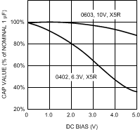 Figure 27. Capacitance vs DC Bias
As shown in Figure 27, increasing the DC bias condition can result in the capacitance value that falls below the minimum value given in the recommended capacitor specifications table. Note that the graph shows the capacitance out of spec for the 0402 case size capacitor at higher bias voltages. It is therefore recommended that the capacitor manufacturers’ specifications for the nominal value capacitor are consulted for all conditions, as some capacitor sizes (such as 0402) may not be suitable in the actual application.
The ceramic capacitor’s capacitance can vary with temperature. The capacitor type X7R, which operates over a temperature range of −55°C to 125°C, will only vary the capacitance to within ±15%. The capacitor type X5R has a similar tolerance over a reduced temperature range of −55°C to 85°C. Many large value ceramic capacitors, larger than 1 μF are manufactured with Z5U or Y5V temperature characteristics. Their capacitance can drop by more than 50% as the temperature varies from 25°C to 85°C. Therefore X7R is recommended over Z5U and Y5V in applications where the ambient temperature will change significantly above or below 25°C.
Tantalum capacitors are less desirable than ceramic for use as output capacitors because they are more expensive when comparing equivalent capacitance and voltage ratings in the 0.47-μF to 4.7-μF range. Another important consideration is that tantalum capacitors have higher ESR values than equivalent size ceramics. This means that while it may be possible to find a tantalum capacitor with an ESR value within the stable range, it would have to be larger in capacitance (which means bigger and more costly) than a ceramic capacitor with the same ESR value. It should also be noted that the ESR of a typical tantalum will increase about 2:1 as the temperature goes from 25°C down to −40°C, so some guard band must be allowed.
Table 8. Capacitor Characteristics
| CAPACITOR | MIN VALUE (µF) | DESCRIPTION | RECOMMENDED TYPE |
|---|---|---|---|
| CLDO1 | 0.47 | LDO1 output capacitor | Ceramic, 6.3V, X5R |
| CLDO2 | 0.47 | LDO2 output capacitor | |
| CSW1 | 10 | SW1 output capacitor | |
| CSW2 | 10 | SW2 output capacitor |
9.2.3 Application Curves
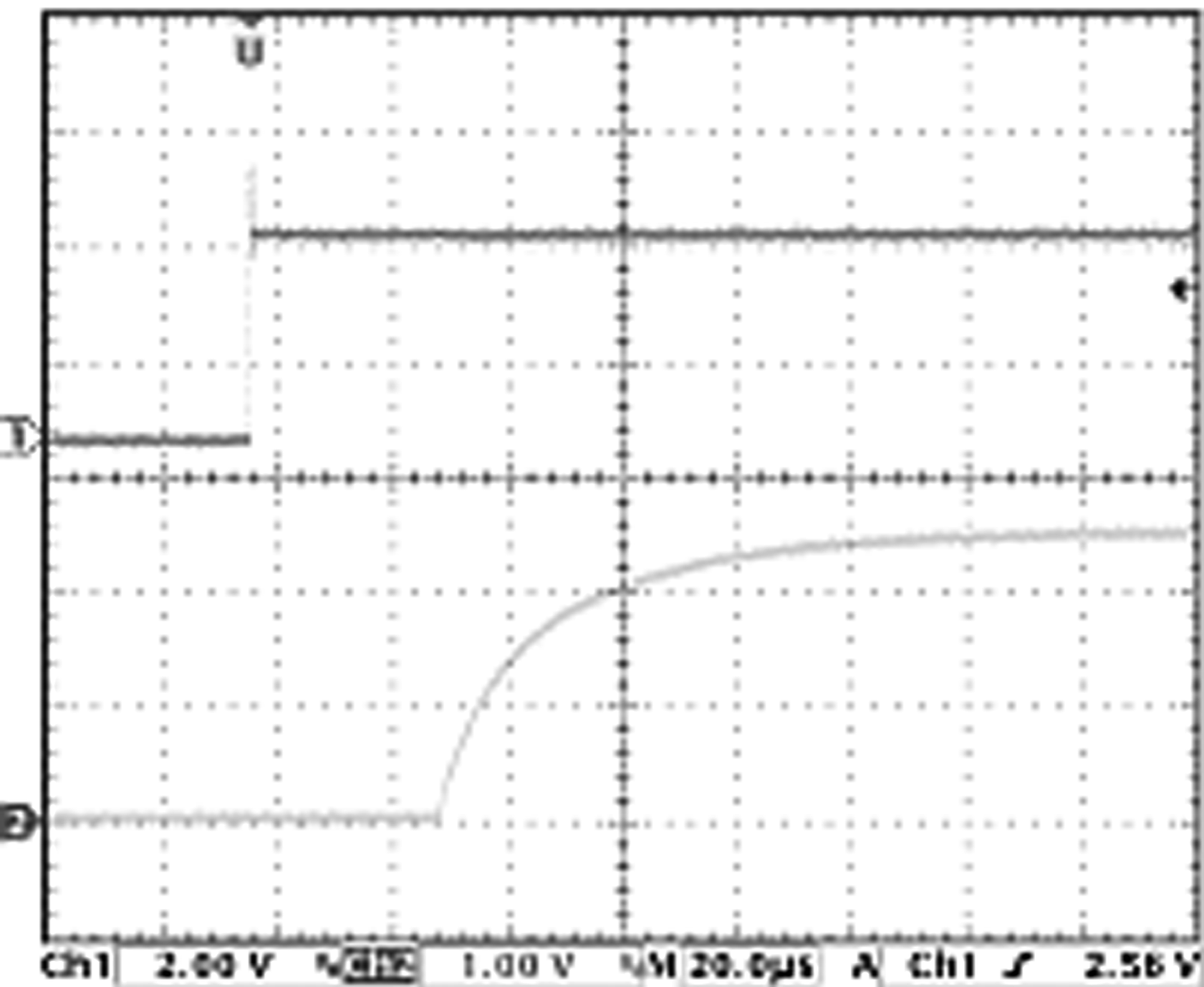
| VIN = 0 to 3.6 V | VOUT = 2.5 V | Load = 1 mA |
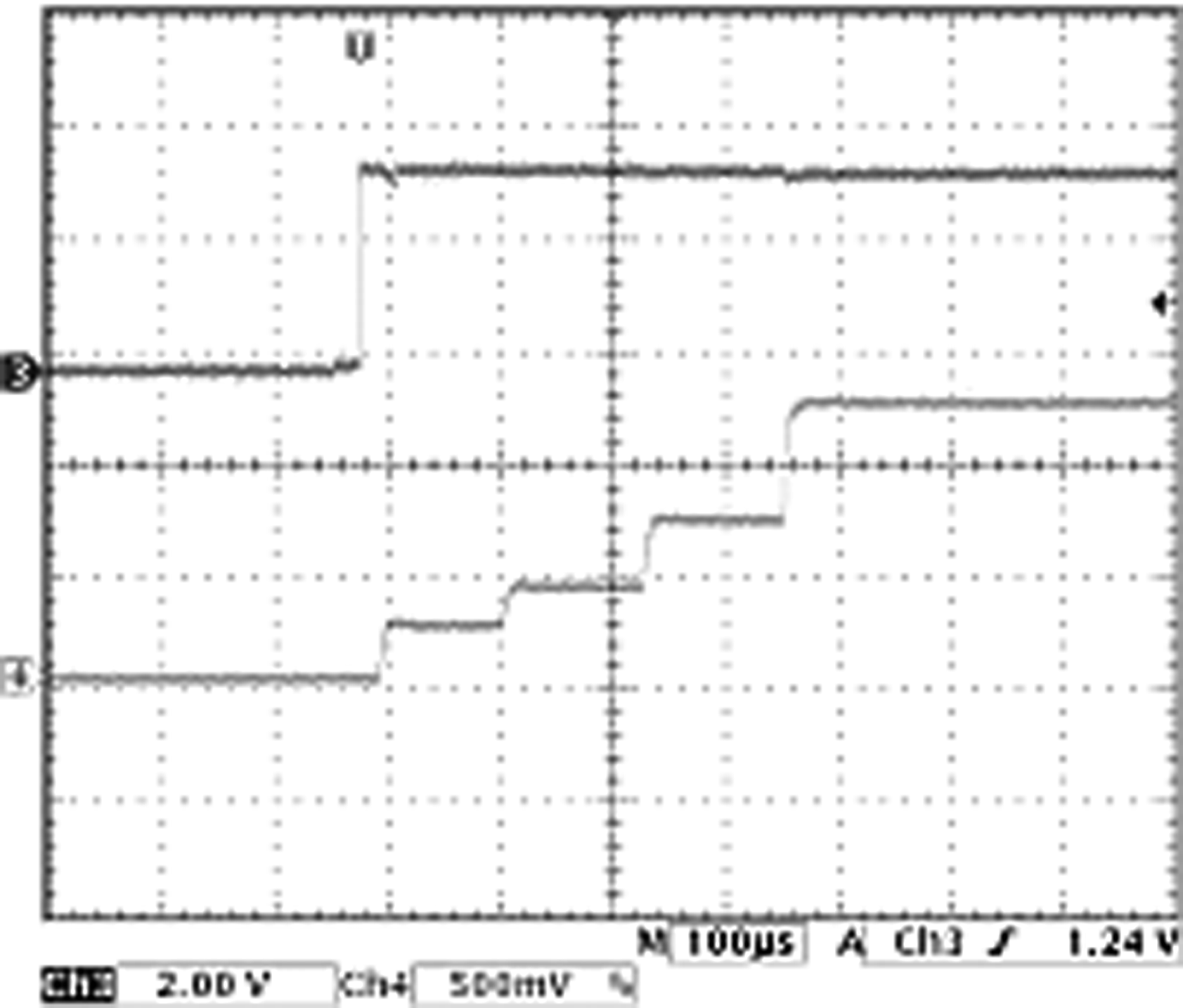
| VIN = 1.2 V | Load = 1.5 A | |
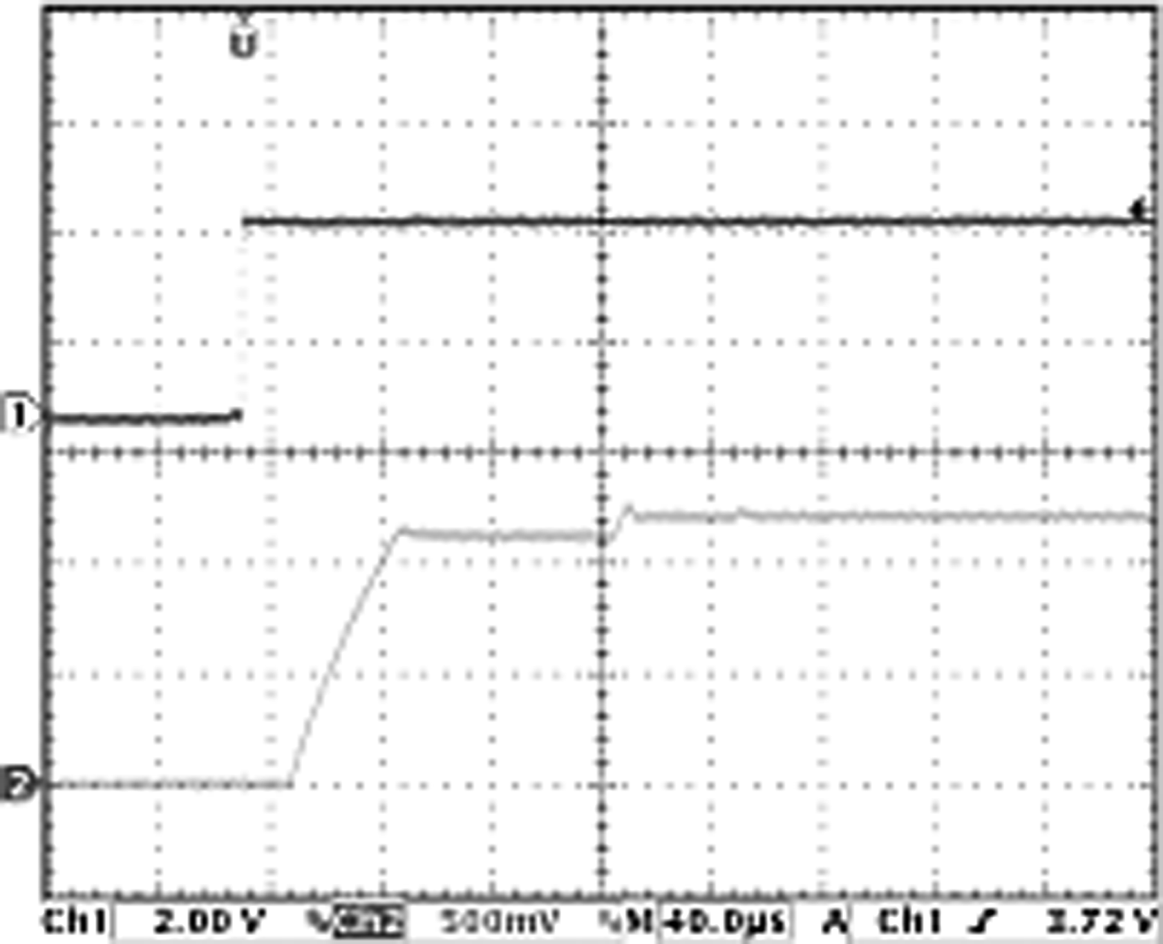
| VIN = 1.2 V | Load = 30 mA | |
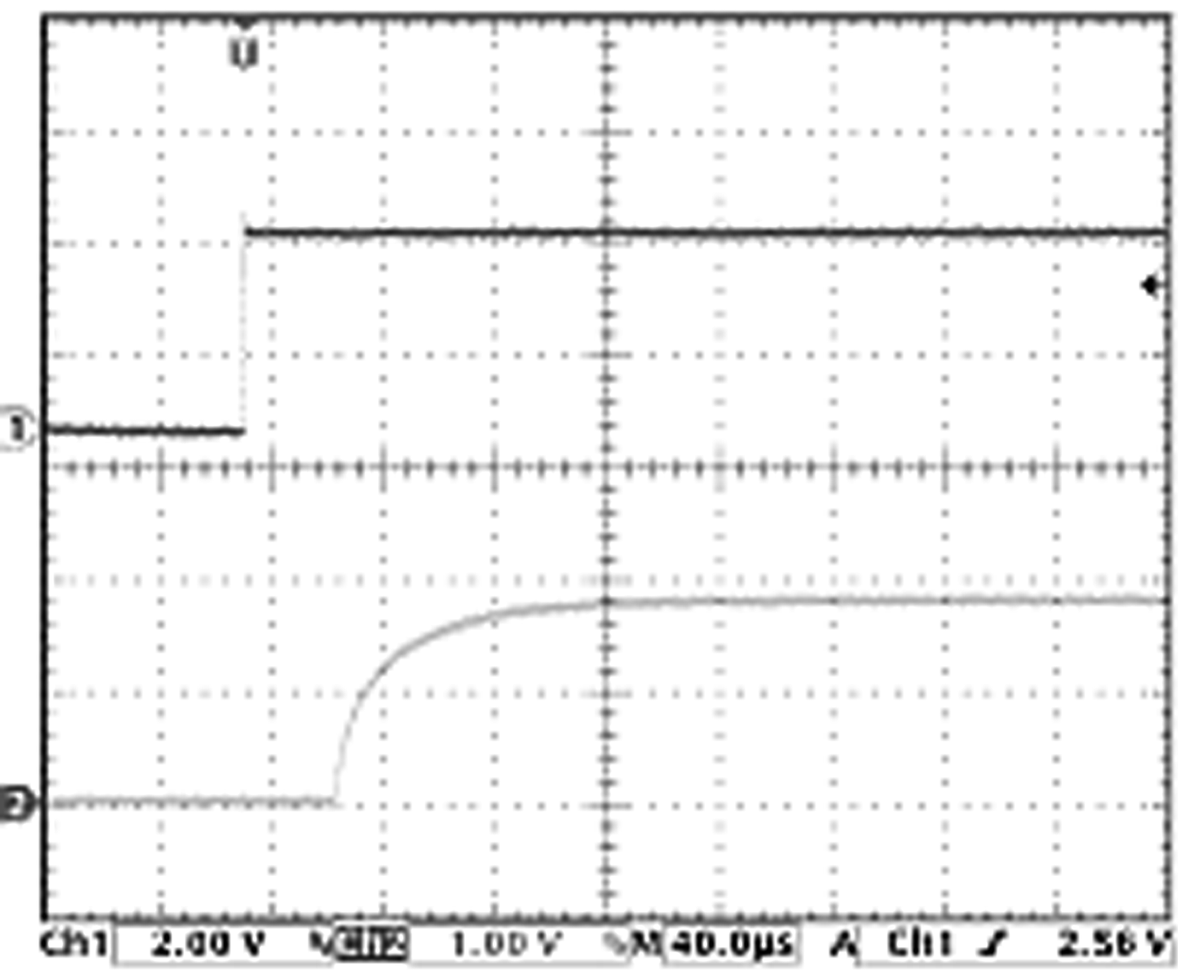
| VIN = 0 to 3.6 V | VOUT = 1.8 V | Load = 1 mA |
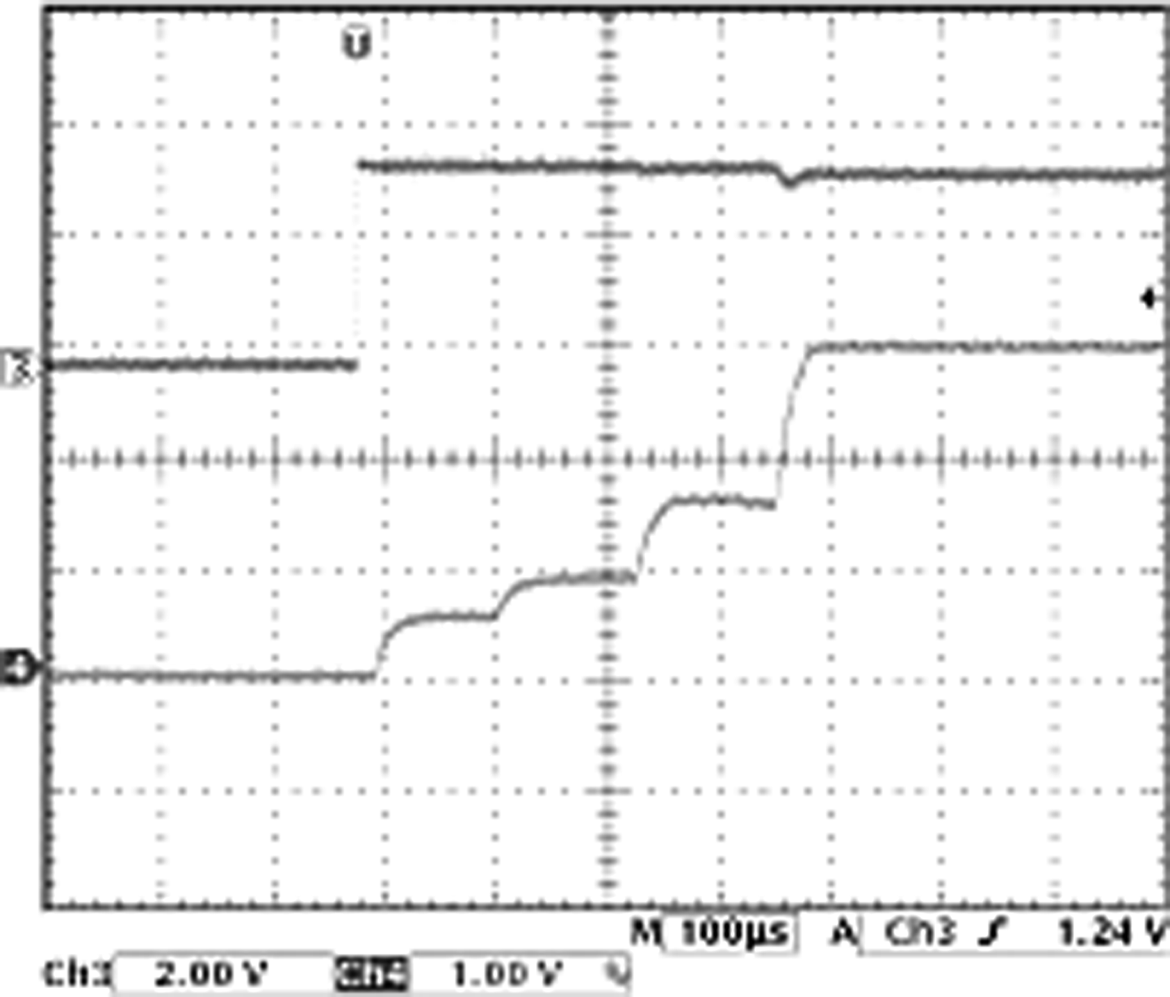
| VIN = 3 V | Load = 1.5 A | |
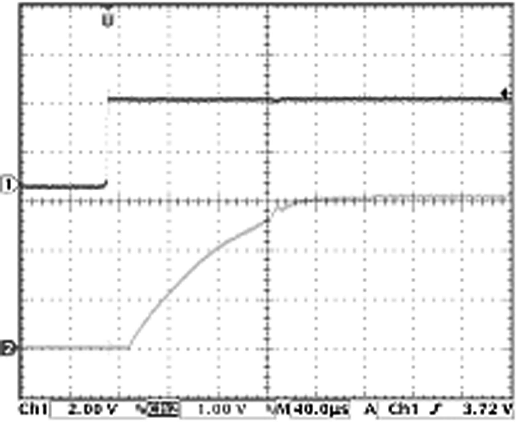
| VIN = 3 V | Load = 30 mA | |
