ZHCSRY0M april 2000 – may 2023 LM2676
PRODUCTION DATA
- 1
- 1 特性
- 2 应用
- 3 说明
- 4 Revision History
- 5 Pin Configuration and Functions
-
6 Specifications
- 6.1 Absolute Maximum Ratings
- 6.2 ESD Ratings
- 6.3 Recommended Operating Conditions
- 6.4 Thermal Information
- 6.5 Electrical Characteristics: LM2676 – 3.3 V
- 6.6 Electrical Characteristics: LM2676 – 5 V
- 6.7 Electrical Characteristics: LM2676 – 12 B
- 6.8 Electrical Characteristics: LM2676 – Adjustable
- 6.9 Electrical Characteristics – All Output Voltage Versions
- 6.10 Typical Characteristics
- 7 Detailed Description
- 8 Application and Implementation
- 9 Device and Documentation Support
- 10Mechanical, Packaging, and Orderable Information
封装选项
机械数据 (封装 | 引脚)
散热焊盘机械数据 (封装 | 引脚)
- KTW|7
订购信息
6.10 Typical Characteristics
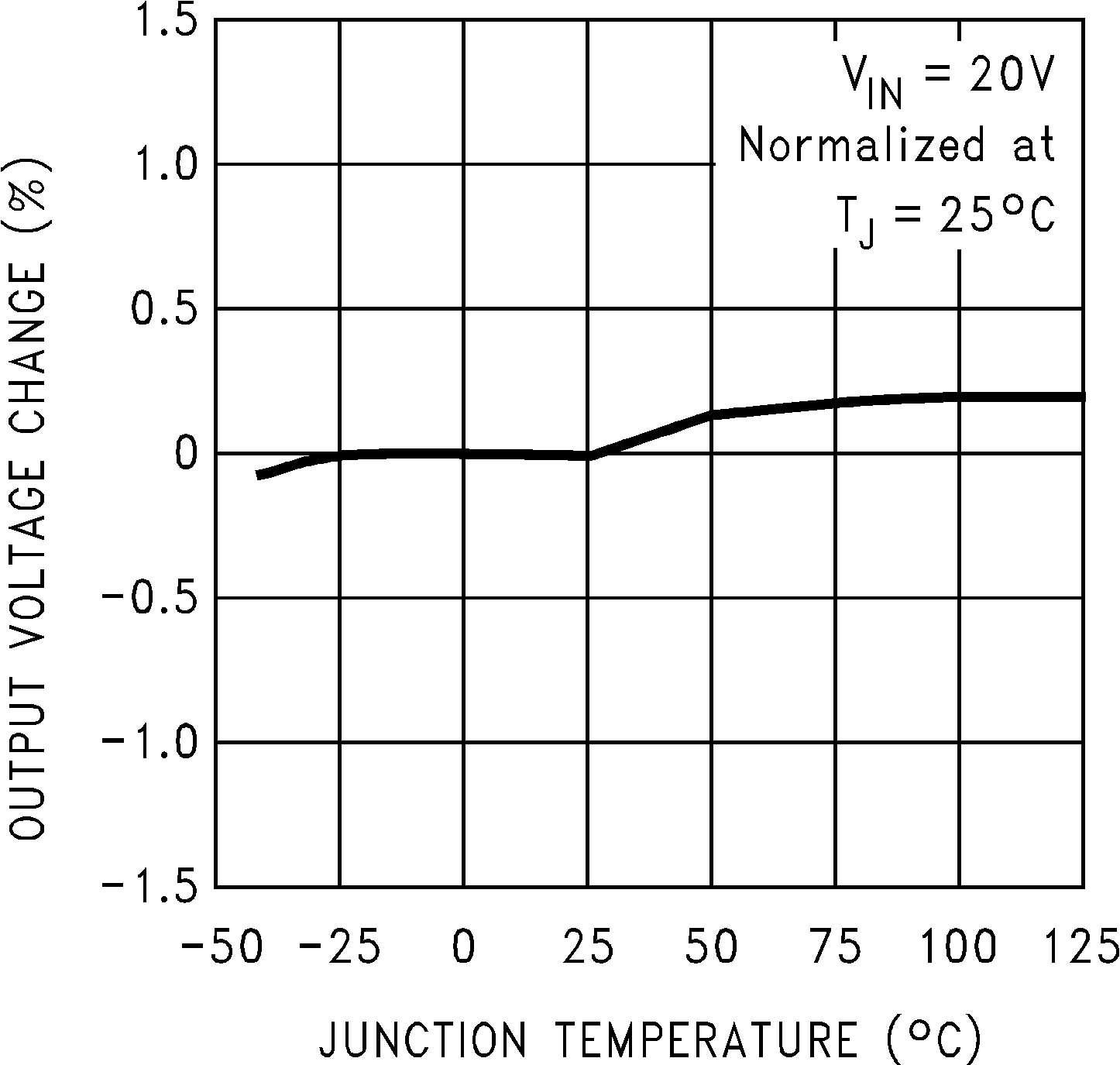 Figure 6-1 Normalized Output Voltage
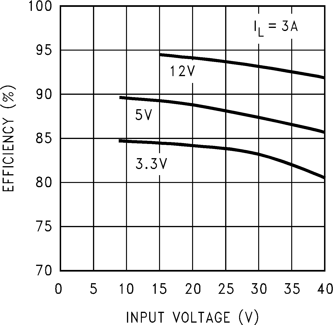 Figure 6-3 Efficiency versus Input Voltage
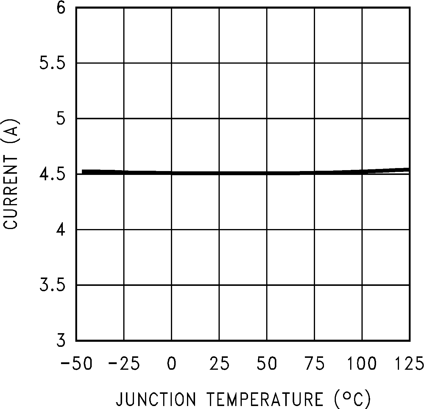 Figure 6-5 Switch Current Limit
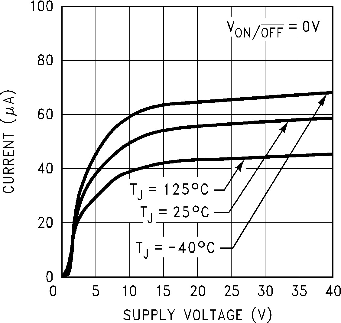 Figure 6-7 Standby Quiescent Current
 Figure 6-9 ON/
OFF Pin Current (Sourcing)
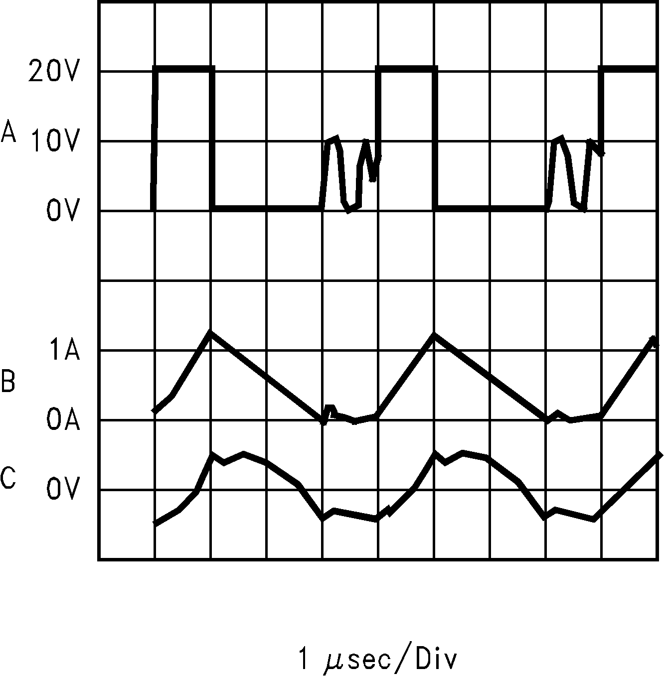
| Discontinuous Mode Switching Waveforms VIN = 20 V, VOUT = 5 V, ILOAD = 500 mA L = 10 µH, COUT = 400 µF, COUTESR = 13 mΩ | ||
| A: VSW Pin Voltage, 10 V/div. | ||
| B: Inductor Current, 1 A/div | ||
| C: Output Ripple Voltage, 20 mV/div AC-Coupled |
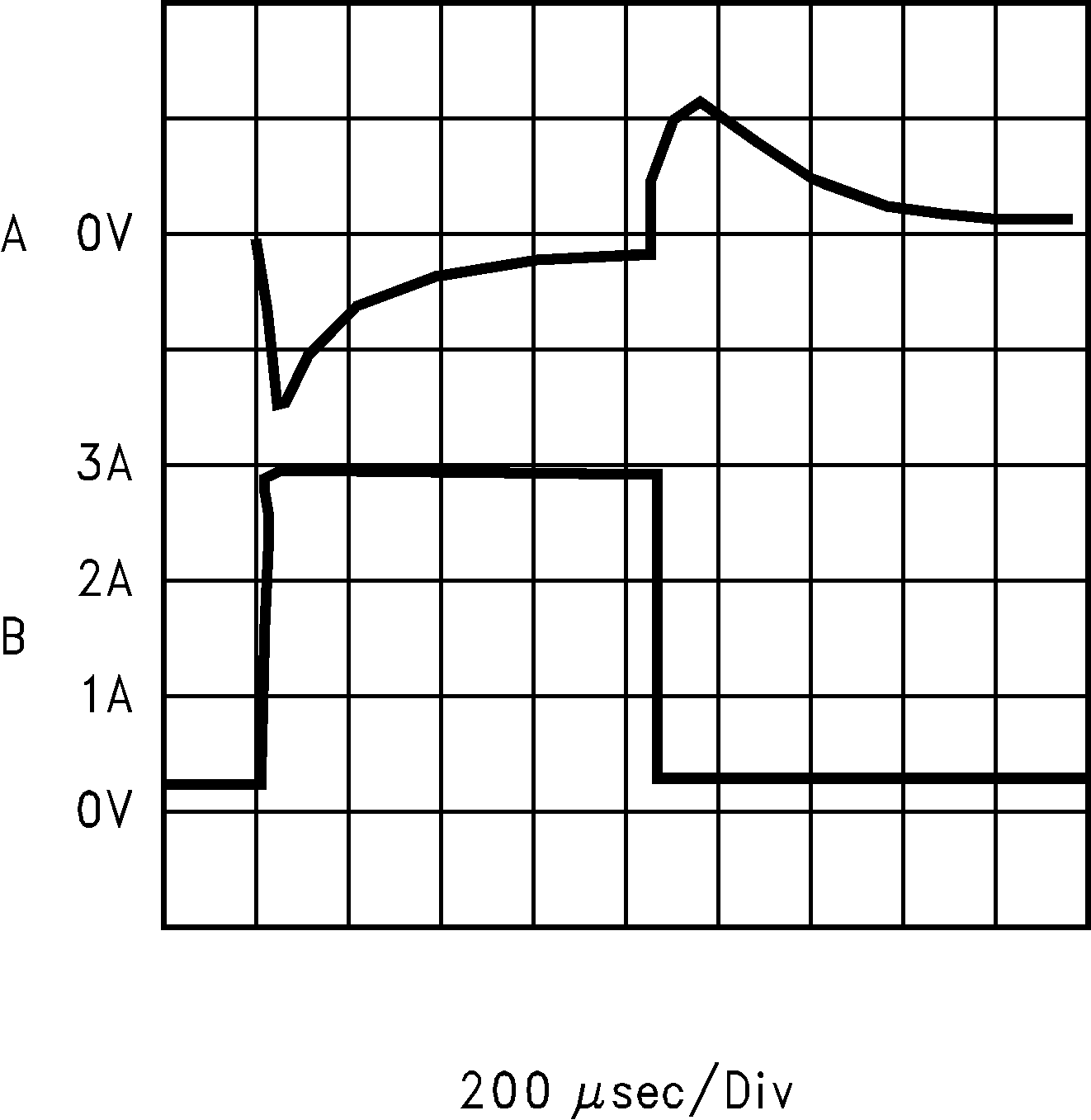
| Load Transient Response for Discontinuous Mode VIN = 20 V, VOUT = 5 V, L = 10 µH, COUT = 400 µF, COUTESR = 13 mΩ | ||
| A: Output Voltage, 100 mV/div, AC-Coupled | ||
| B: Load Current: 200-mA to 3-A Load Pulse |
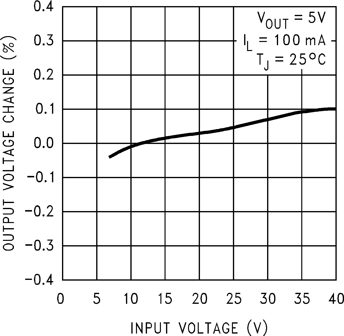 Figure 6-2 Line Regulation
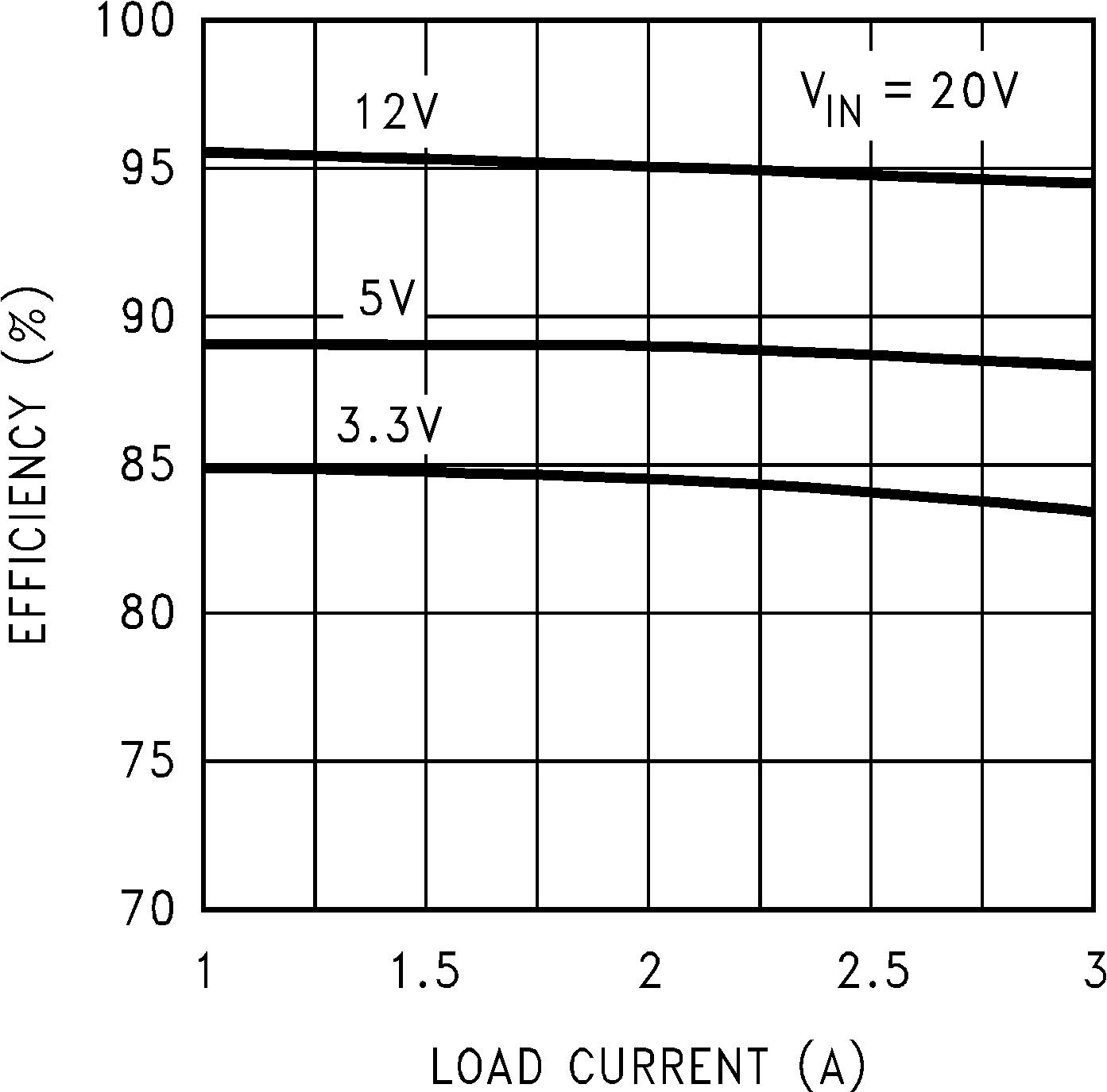 Figure 6-4 Efficiency versus ILOAD
 Figure 6-6 Operating Quiescent Current
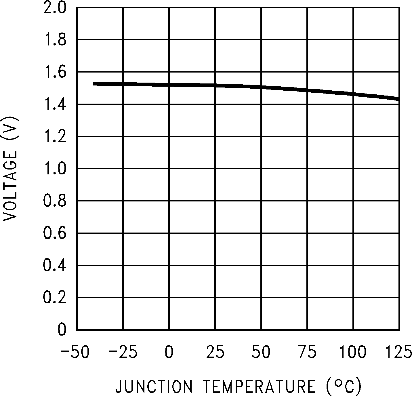 Figure 6-8 ON/OFF Threshold Voltage
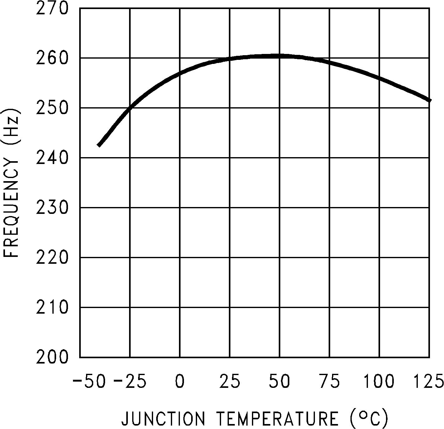 Figure 6-10 Switching Frequency
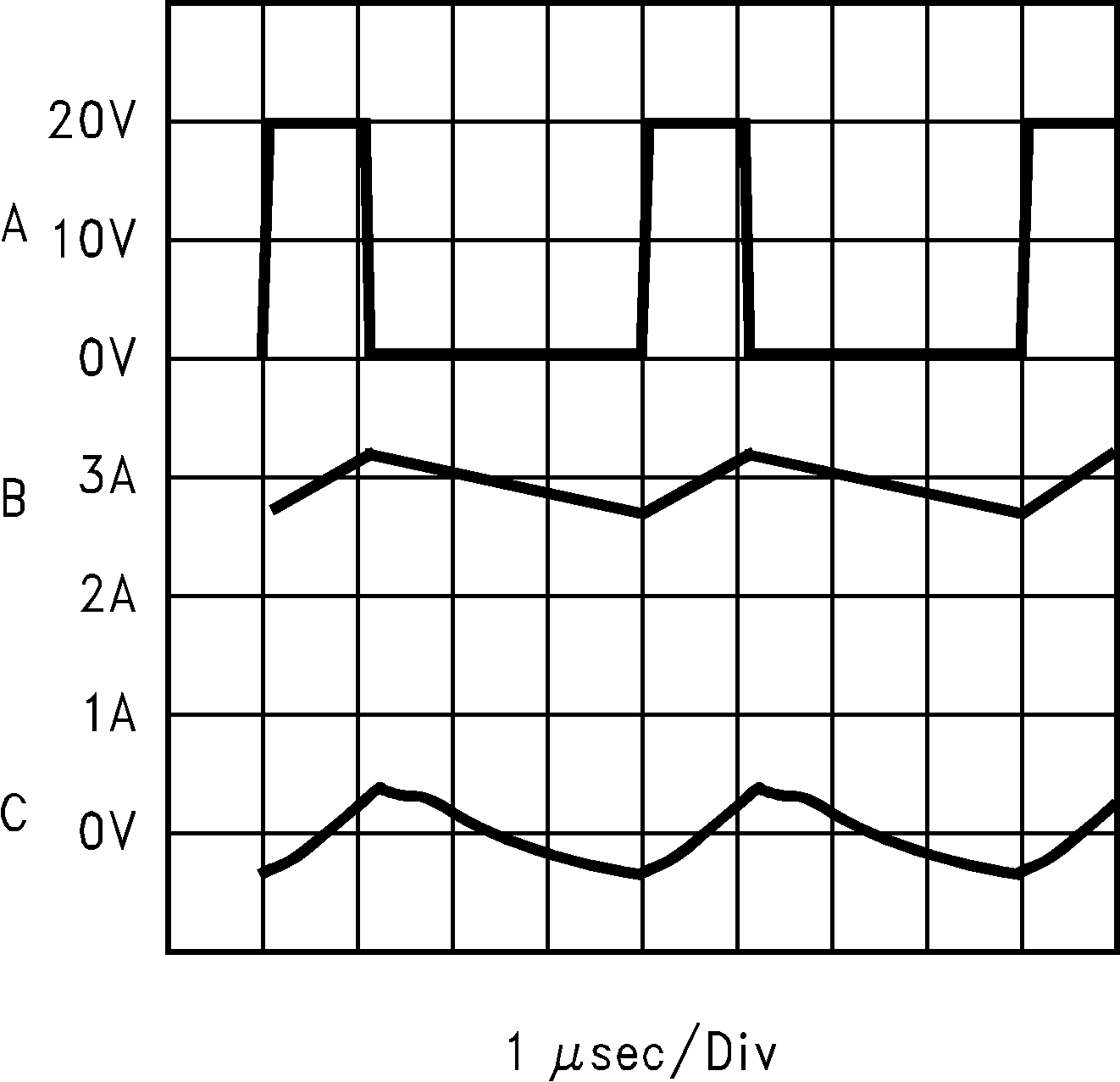
| Continuous Mode Switching Waveforms VIN = 20 V, VOUT = 5 V, ILOAD = 3 A L = 33 µH, COUT = 200 µF, COUTESR = 26 mΩ | ||
| A: VSW Pin Voltage, 10 V/div. | ||
| B: Inductor Current, 1 A/div | ||
| C: Output Ripple Voltage, 20 mV/div AC-Coupled |
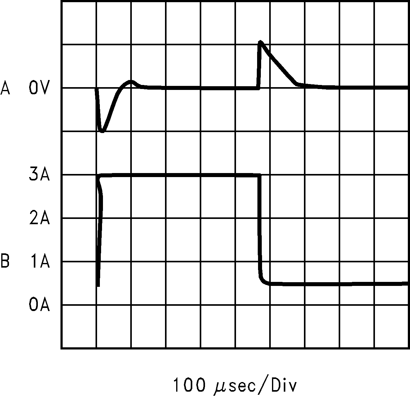
| Load Transient Response for Continuous Mode VIN = 20 V, VOUT = 5 V L = 33 µH, COUT = 200 µF, COUTESR = 26 mΩ | ||
| A: Output Voltage, 100 mV//div, AC-Coupled. | ||
| B: Load Current: 500-mA to 3-A Load Pulse | ||