SNVS153F May 2001 – September 2016 LM2698
PRODUCTION DATA.
- 1 Features
- 2 Applications
- 3 Description
- 4 Revision History
- 5 Pin Configuration and Functions
- 6 Specifications
- 7 Detailed Description
- 8 Application and Implementation
- 9 Power Supply Recommendations
- 10Layout
- 11Device and Documentation Support
- 12Mechanical, Packaging, and Orderable Information
7 Detailed Description
7.1 Overview
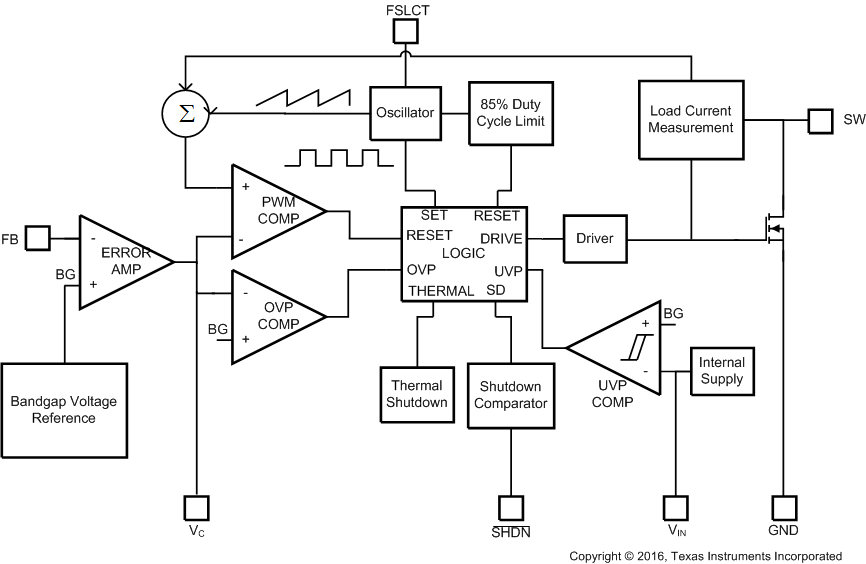
The LM2698 is a boost controller with integrated primary switch. The LM2698 functions in current mode control by sensing the current into the integrated switch and adding a slope to the signal for slope compensation purpose. The device provides a cycle by cycle current limiting and the duty cycle is limited to 85% to ensure an additional level of protection. A frequency selection pin FSLCT allows the designer to choose between two switching frequencies (600 kHz or 1250 kHz). A shutdown pin is available to suspend the device and decrease the quiescent current to 5 µA by pulling the pin to a logic high.
7.2 Functional Block Diagram

7.3 Feature Description
7.3.1 Inductor
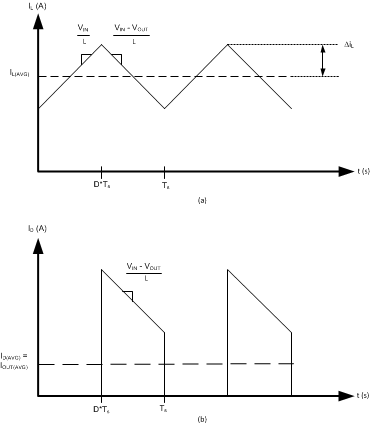
The inductor is one of the two energy storage elements in a boost converter. Figure 13 shows how the inductor current varies during a switching cycle. The current through an inductor is quantified with Equation 1.
 Figure 13. (a) Inductor Current (b) Diode Current

If VL(t) is constant, diL / dt must be constant, thus the current in the inductor changes at a constant rate. This is the case in DC/DC converters since the voltages at the input and output can be approximated as a constant. The current through the inductor of the LM2698 boost converter is shown in Figure 13(a). The important quantities in determining a proper inductance value are IL(AVG) (the average inductor current) and ΔiL (the inductor current ripple). If ΔiL is larger than IL(AVG), the inductor current drops to zero for a portion of the cycle and the converter operates in discontinuous conduction mode. If ΔiL is smaller than IL(AVG), the inductor current stays above zero and the converter operates in continuous conduction mode (CCM). All the analysis in this datasheet assumes operation in continuous conduction mode. To operate in CCM, use Equation 2, Equation 3, and Equation 4.


Choose the minimum IOUT to determine the minimum L for CCM operation. A common choice is to set ΔiL to 30% of IL(AVG).
The inductance value also affects the stability of the converter. Because the LM2698 utilizes current mode control, the inductor value must be carefully chosen. See Compensation for recommended inductance values.
Choosing an appropriate core size for the inductor involves calculating the average and peak currents expected through the inductor. In a boost converter, use Equation 5 and Equation 6 (where Equation 7 calculates ΔiL).
 ,
, 
A core size with ratings higher than these values must be chosen. If the core is not properly rated, saturation dramatically reduces overall efficiency.
7.3.2 Current Limit
The current limit in the LM2698 is referenced to the peak switch current. The peak currents in the switch of a boost converter is always higher than the average current supplied to the load. To determine the maximum average output current that the LM2698 can supply, use Equation 8.
where
- ICL is the switch current limit (see Electrical Characteristics)
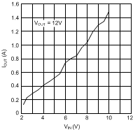
Hence, as VIN increases, the maximum current that can be supplied to the load increases, as shown in Figure 14.
 Figure 14. Maximum Output Current vs Input Voltage
7.3.3 Diode
The diode in a boost converter such as the LM2698 acts as a switch to the output. During the first cycle, when the transistor is closed, the diode is reverse biased and current is blocked; the load current is supplied by the output capacitor. In the second cycle, the transistor is open and the diode is forward biased; the load current is supplied by the inductor.
Observation of the boost converter circuit shows that the average current through the diode is the average load current, and the peak current through the diode is the peak current through the inductor. The diode must be rated to handle more than its peak current. To improve efficiency, a low forward drop Schottky diode is recommended.
7.3.4 Input Capacitor
Due to the presence of an inductor at the input of a boost converter, the input current waveform is continuous and triangular. The inductor ensures that the input capacitor sees fairly low ripple currents. However, as the inductor gets smaller, the input ripple increases. The rms current in the input capacitor is given by Equation 9.

The input capacitor must be capable of handling the rms current. Although the input capacitor is not so critical in boost applications, a 10 µF or higher value, good quality capacitor prevents any impedance interactions with the input supply.
A 0.1-µF or 1-µF ceramic bypass capacitor is also recommended on the VIN pin (pin 6) of the IC. This capacitor must be connected very close to pin 6 to effectively filter high frequency noise. When operating at 1.25-MHz switching frequency, a minimum bypass capacitance of 0.22 µF is recommended.
7.3.5 Output Capacitor
The output capacitor in a boost converter provides all the output current when the switch is closed and the inductor is charging. As a result, it sees very large ripple currents. The output capacitor must be capable of handling the maximum RMS current. The RMS current in the output capacitor is calculated with Equation 10 (where Equation 11 calculates ΔiL).

where
- D = (VOUT – VIN) / VOUT

The ESR and ESL of the output capacitor directly control the output ripple. Use capacitors with low ESR and ESL at the output for high efficiency and low ripple voltage. Surface mount tantalums, surface mount polymer electrolytic, and polymer tantalum, Sanyo OS-CON, or multi-layer ceramic capacitors are recommended at the output.
7.4 Device Functional Modes
7.4.1 Continuous Conduction Mode
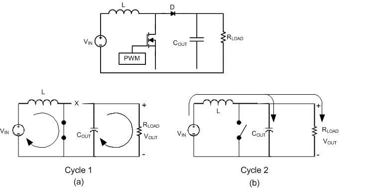
 Figure 15. Simplified Boost Converter Diagram
(a) First Cycle of Operation (b) Second Cycle Of Operation
The LM2698 is a current-mode, PWM boost regulator. A boost regulator steps the input voltage up to a higher output voltage. In continuous conduction mode (when the inductor current never reaches zero at steady state), the boost regulator operates in two cycles.
In the first cycle of operation, shown in Figure 15 (a), the transistor is closed and the diode is reverse biased. Energy is collected in the inductor and the load current is supplied by COUT.
The second cycle is shown in Figure 15 (b). During this cycle, the transistor is open and the diode is forward biased. The energy stored in the inductor is transferred to the load and output capacitor.
The ratio of these two cycles determines the output voltage. The output voltage is defined with Equation 12.

where
- D is the duty cycle of the switch