SNVS153F May   2001  – September 2016 LM2698

PRODUCTION DATA.  

  1. Features
  2. Applications
  3. Description
  4. Revision History
  5. Pin Configuration and Functions
  6. Specifications
    1. 6.1 Absolute Maximum Ratings
    2. 6.2 ESD Ratings
    3. 6.3 Recommended Operating Conditions
    4. 6.4 Thermal Information
    5. 6.5 Electrical Characteristics
    6. 6.6 Typical Characteristics
  7. Detailed Description
    1. 7.1 Overview
    2. 7.2 Functional Block Diagram
    3. 7.3 Feature Description
      1. 7.3.1 Inductor
      2. 7.3.2 Current Limit
      3. 7.3.3 Diode
      4. 7.3.4 Input Capacitor
      5. 7.3.5 Output Capacitor
    4. 7.4 Device Functional Modes
      1. 7.4.1 Continuous Conduction Mode
  8. Application and Implementation
    1. 8.1 Application Information
    2. 8.2 Typical Applications
      1. 8.2.1 1.25-MHz Boost Converter
        1. 8.2.1.1 Design Requirements
        2. 8.2.1.2 Detailed Design Procedure
          1. 8.2.1.2.1 Compensation
            1. 8.2.1.2.1.1 Quick Compensator Design
            2. 8.2.1.2.1.2 Improving Transient Response Time
            3. 8.2.1.2.1.3 Additional Comments on the Open Loop Frequency Response
        3. 8.2.1.3 Application Curves
      2. 8.2.2 3.3-V SEPIC
        1. 8.2.2.1 Design Requirements
        2. 8.2.2.2 Detailed Design Procedure
        3. 8.2.2.3 Application Curve
      3. 8.2.3 Level-Shifted SEPIC
        1. 8.2.3.1 Design Requirements
  9. Power Supply Recommendations
  10. 10Layout
    1. 10.1 Layout Guidelines
    2. 10.2 Layout Examples
  11. 11Device and Documentation Support
    1. 11.1 Receiving Notification of Documentation Updates
    2. 11.2 Community Resources
    3. 11.3 Trademarks
    4. 11.4 Electrostatic Discharge Caution
    5. 11.5 Glossary
  12. 12Mechanical, Packaging, and Orderable Information

封装选项

机械数据 (封装 | 引脚)
散热焊盘机械数据 (封装 | 引脚)
订购信息

10 Layout

10.1 Layout Guidelines

The GND pin and the NC pin is recommended to be connected by a short trace as shown in Layout Examples.

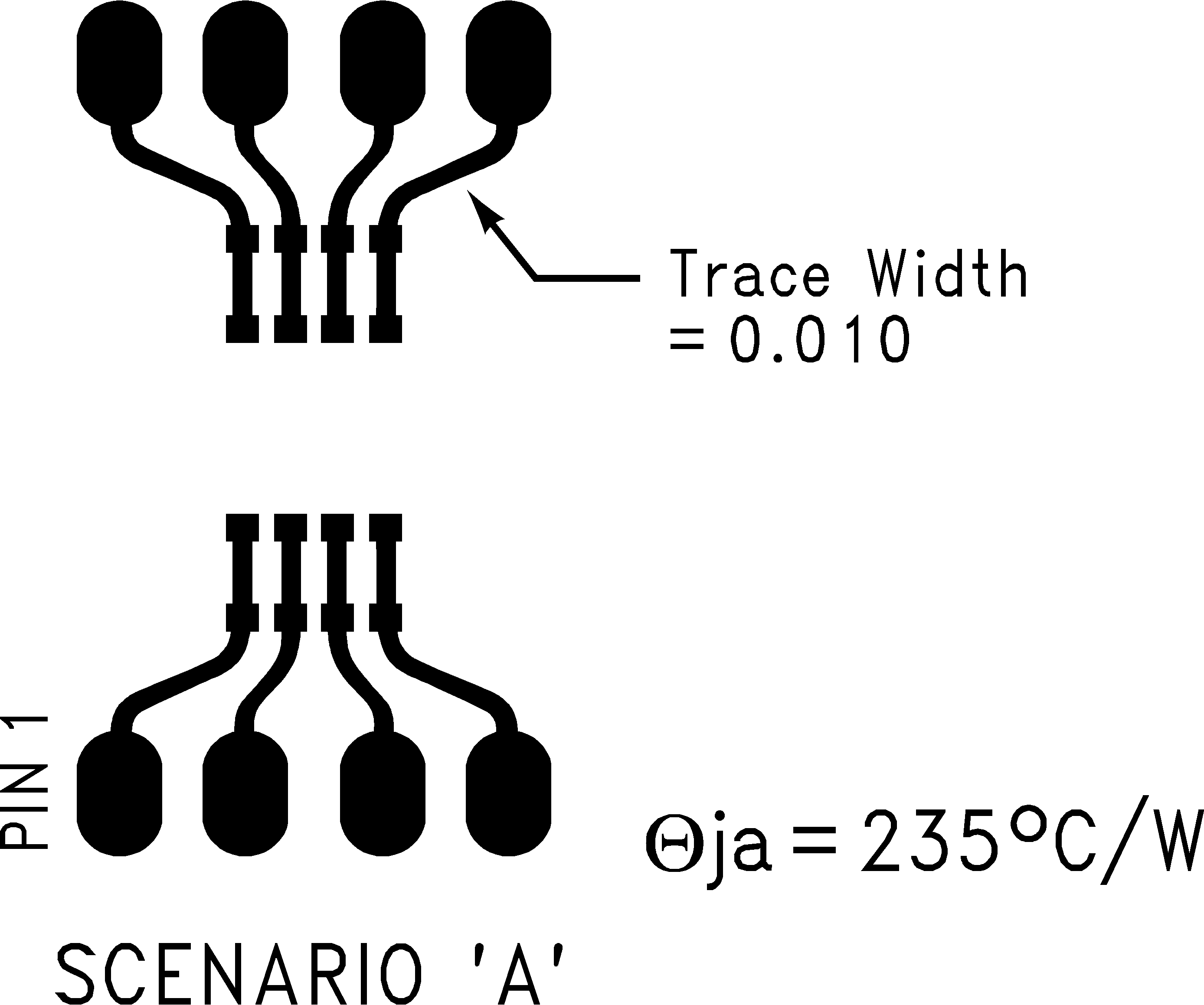
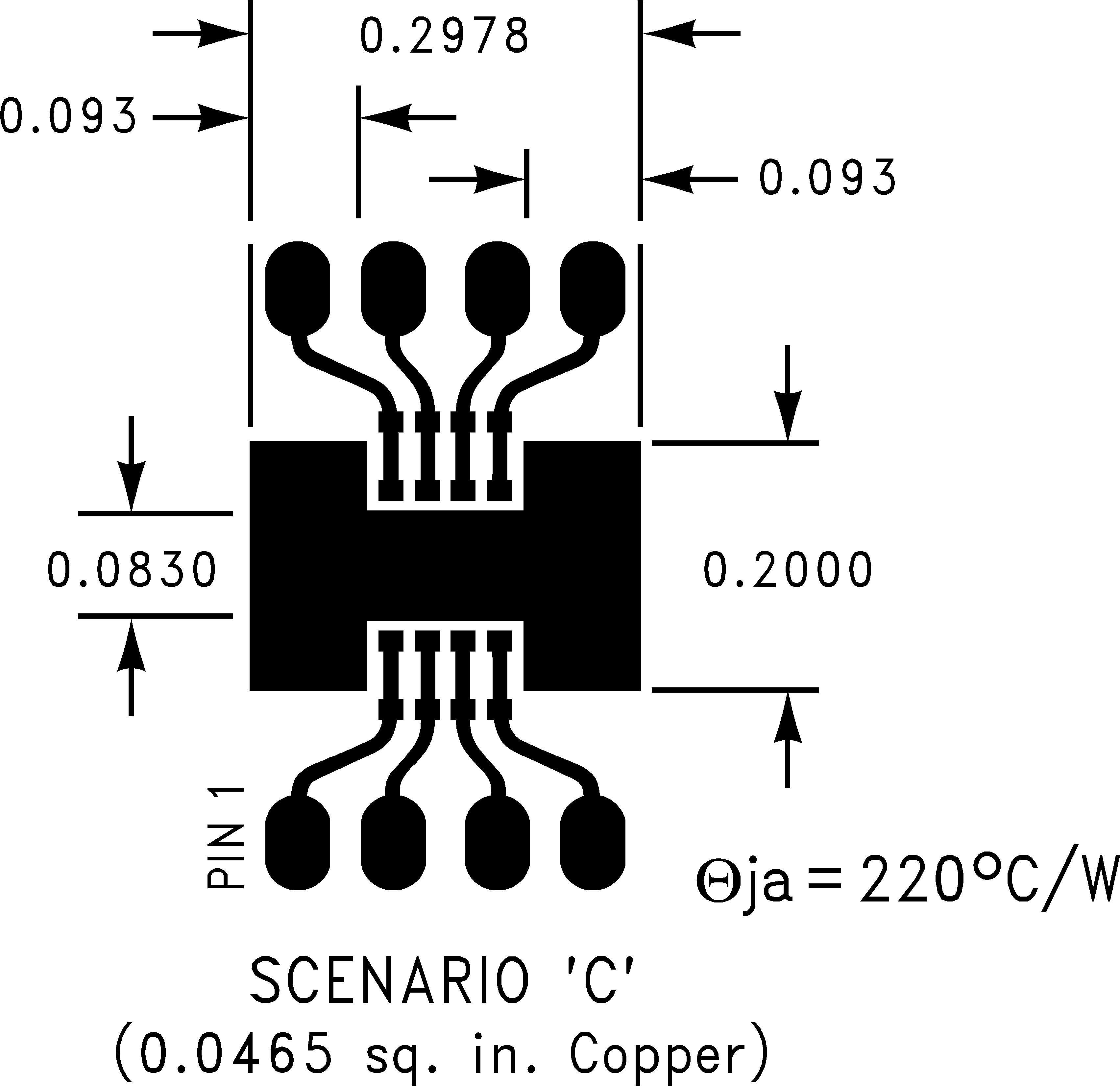
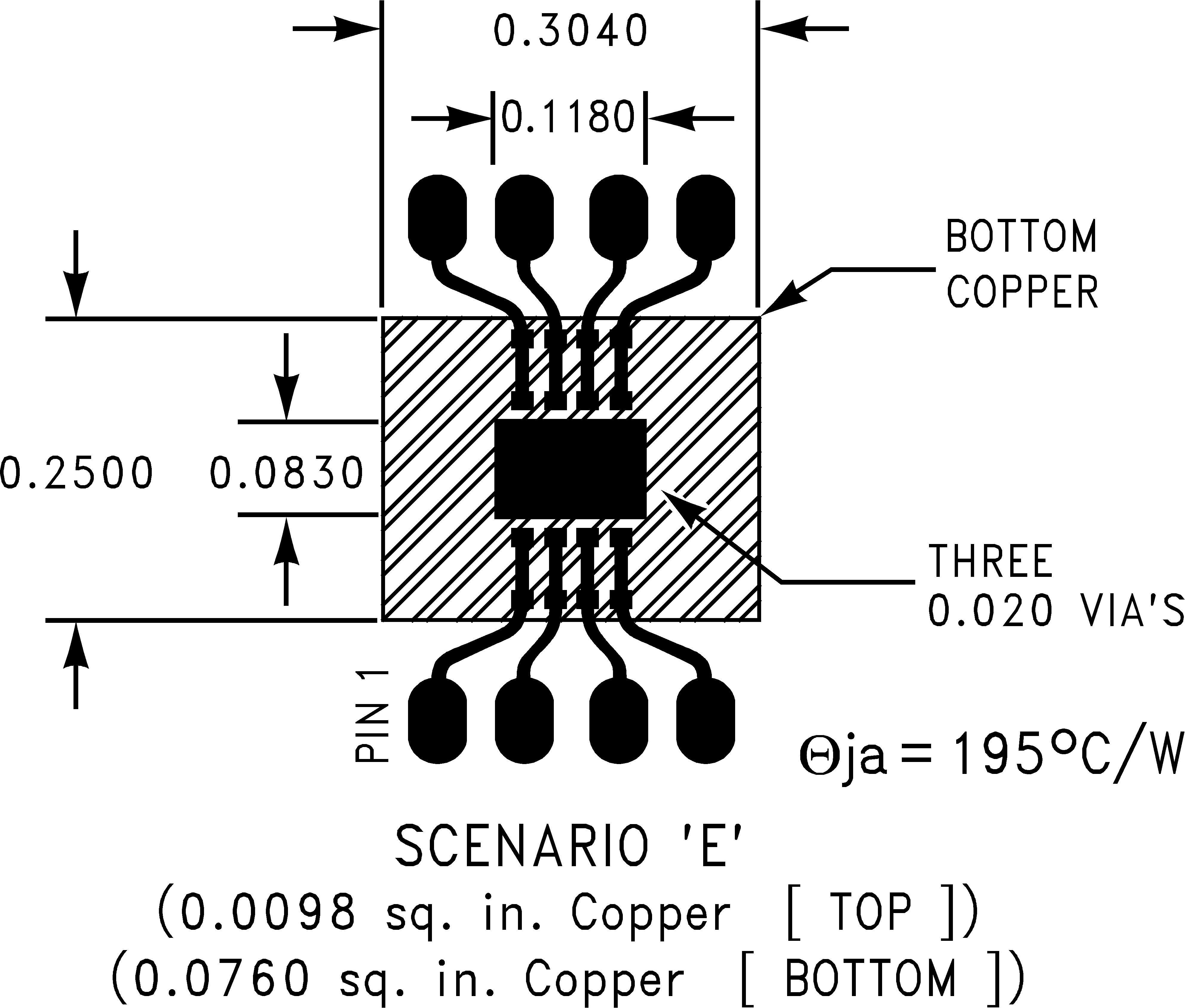
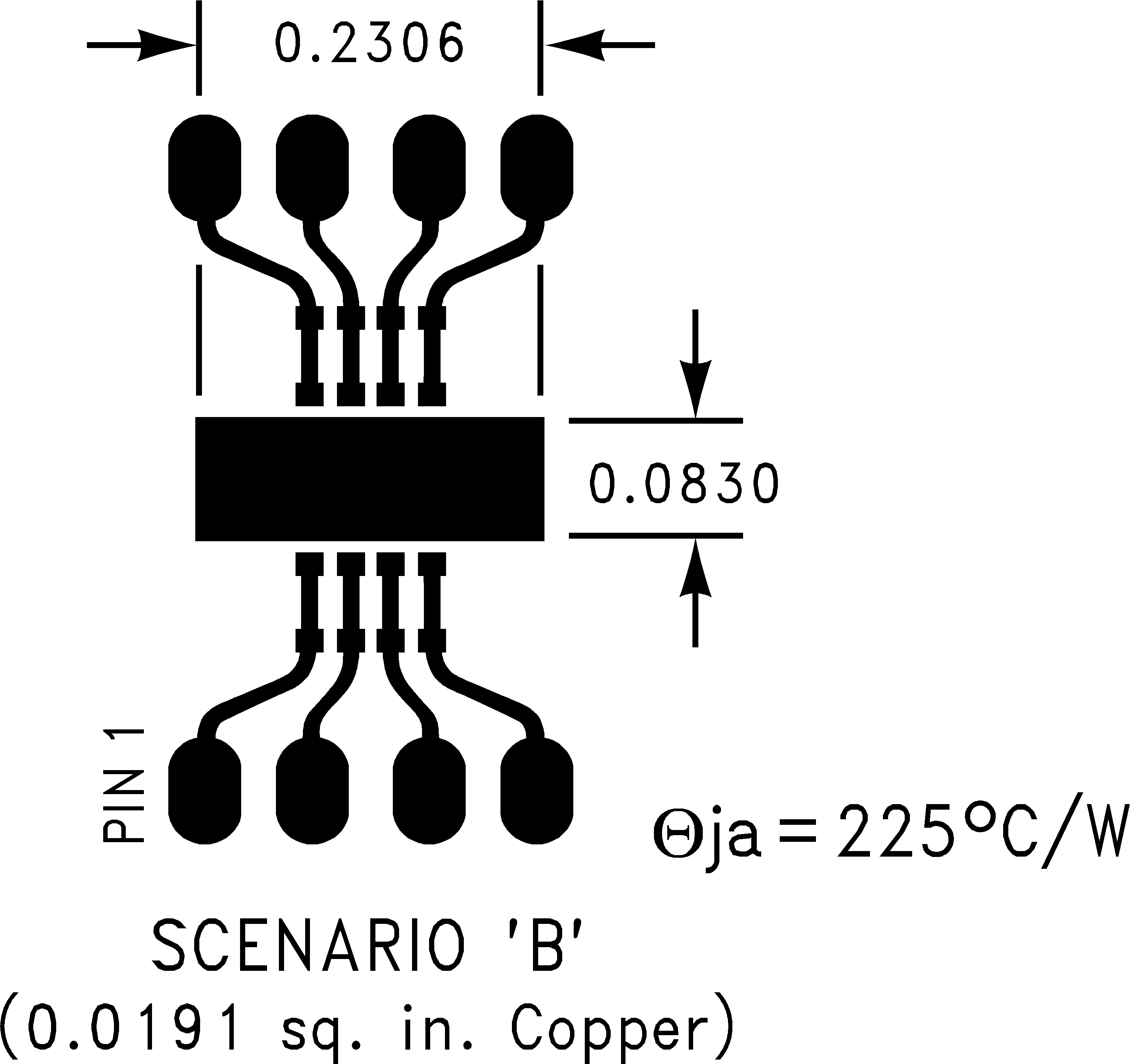
Table 2 shows the thermal resistance using different scenarios.

Table 2. Thermal Resistance

PARAMETER TYP UNIT
θJA Thermal Resistance Junction to Ambient Figure 25 235 °C/W
Junction to Ambient Figure 26 225 °C/W
Junction to Ambient Figure 27 220 °C/W
Junction to Ambient Figure 28 200 °C/W
Junction to Ambient Figure 29 195 °C/W

10.2 Layout Examples

LM2698 20012611.png
Junction to ambient thermal resistance (no external heat sink) for the MSO8 package with minimal trace widths (0.010 inches) from the pins to the circuit.
Figure 25. Pad Layout Scenario 'A'
LM2698 20012613.png
Junction to ambient thermal resistance for the MSO8 package with minimal trace widths (0.010 inches) from the pins to the circuit and approximately 0.0465 sq. in. of copper heat sinking.
Figure 27. Pad Layout Scenario 'C'
LM2698 20012615.png
Junction to ambient thermal resistance for the MSO8 package with minimal trace widths (0.010 inches) from the pins to the circuit and approximately 0.0098 sq. in. of copper heat sinking on the top layer and 0.0760 sq. in. of copper heat sinking on the bottom layer, with three 0.020 in. vias connecting the planes.
Figure 29. Pad Layout Scenario 'E'
LM2698 20012612.png
Junction to ambient thermal resistance for the MSO8 package with minimal trace widths (0.010 inches) from the pins to the circuit and approximately 0.0191 sq. in. of copper heat sinking.
Figure 26. Pad Layout Scenario 'B'
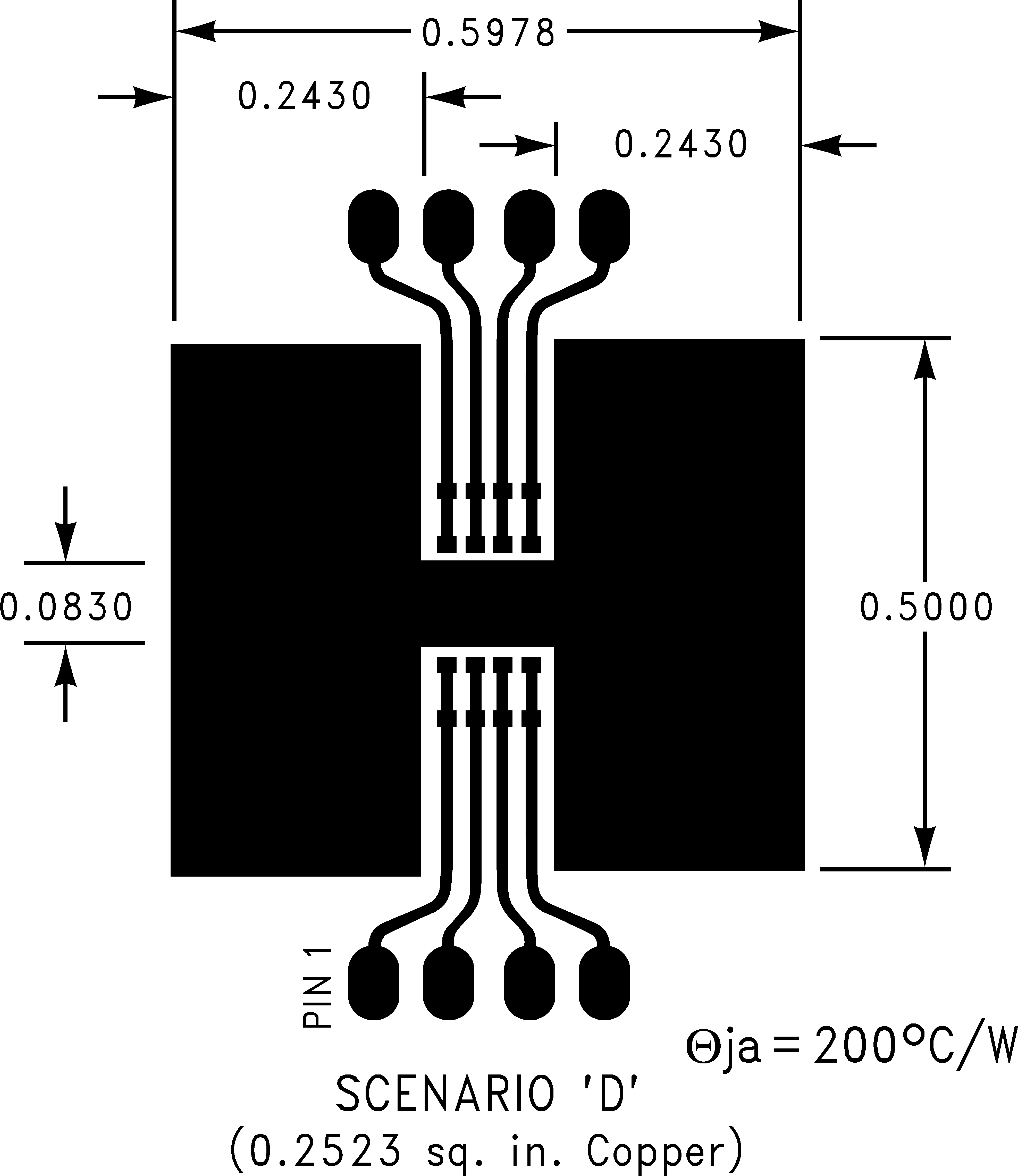
LM2698 20012614.png
Junction to ambient thermal resistance for the MSO8 package with minimal trace widths (0.010 inches) from the pins to the circuit and approximately 0.2523 sq. in. of copper heat sinking.
Figure 28. Pad Layout Scenario 'D'