SNIS144G July 2007 – September 2016 LM26LV , LM26LV-Q1
PRODUCTION DATA.
- 1 Features
- 2 Applications
- 3 Description
- 4 Revision History
- 5 Pin Configuration and Functions
- 6 Specifications
-
7 Detailed Description
- 7.1 Overview
- 7.2 Functional Block Diagram
- 7.3 Feature Description
- 7.4 Device Functional Modes
- 8 Application and Implementation
- 9 Power Supply Recommendations
- 10Layout
- 11Device and Documentation Support
- 12Mechanical, Packaging, and Orderable Information
6 Specifications
6.1 Absolute Maximum Ratings
over operating free-air temperature range (unless otherwise noted)(1)(3)| MIN | MAX | UNIT | |
|---|---|---|---|
| Supply voltage | –0.3 | 6 | V |
| Voltage at OVERTEMP pin | –0.3 | 6 | V |
| Voltage at OVERTEMP and VTEMP pins | –0.3 | VDD + 0.5 | V |
| TRIP_TEST input voltage | –0.3 | VDD + 0.5 | V |
| Output current, any output pin | –7 | 7 | mA |
| Input current at any pin(2) | 5 | mA | |
| Maximum junction temperature, TJ(MAX) | 155 | °C | |
| Storage temperature, Tstg | –65 | 150 | °C |
(1) Stresses beyond those listed under Absolute Maximum Ratings may cause permanent damage to the device. These are stress ratings only, which do not imply functional operation of the device at these or any other conditions beyond those indicated under Recommended Operating Conditions. Exposure to absolute-maximum-rated conditions for extended periods may affect device reliability.
(2) When the input voltage (VI) at any pin exceeds power supplies (VI < GND or VI > VDD), the current at that pin must be limited to 5 mA.
(3) For soldering specifications, see Absolute Maximum Ratings for Soldering.
6.2 ESD Ratings: LM26LV
| VALUE | UNIT | |||
|---|---|---|---|---|
| V(ESD) | Electrostatic discharge | Human-body model (HBM), per ANSI/ESDA/JEDEC JS-001(1) | ±4500 | V |
| Charged-device model (CDM), per JEDEC specification JESD22-C101(2) | ±1000 | |||
| Machine model (MM)(3) | ±300 | |||
(1) JEDEC document JEP155 states that 500-V HBM allows safe manufacturing with a standard ESD control process. Manufacturing with less than 500-V HBM is possible with the necessary precautions.
(2) JEDEC document JEP157 states that 250-V CDM allows safe manufacturing with a standard ESD control process.
(3) The machine model (MM) is a 200-pF capacitor charged to the specified voltage then discharged directly into each pin.
6.3 ESD Ratings: LM26LV-Q1
| VALUE | UNIT | |||
|---|---|---|---|---|
| V(ESD) | Electrostatic discharge | Human-body model (HBM), per AEC Q100-002(1) | ±4500 | V |
| Charged-device model (CDM), per AEC Q100-011 | ±1000 | |||
| Machine model (MM) | ±300 | |||
(1) AEC Q100-002 indicates that HBM stressing shall be in accordance with the ANSI/ESDA/JEDEC JS-001 specification.
6.4 Recommended Operating Conditions
over operating free-air temperature range (unless otherwise noted)| MIN | NOM | MAX | UNIT | ||
|---|---|---|---|---|---|
| VDD | Supply voltage | 1.6 | 5.5 | V | |
| Supply current | 8 | µA | |||
| TA | Specified ambient temperature | –50 | 150 | °C | |
6.5 Thermal Information
| THERMAL METRIC(1) | LM26LV and LM26LV-Q1 | UNIT | |
|---|---|---|---|
| NGF (WSON) | |||
| 6 PINS | |||
| RθJA | Junction-to-ambient thermal resistance | 100.7 | °C/W |
| RθJC(top) | Junction-to-case (top) thermal resistance | 121.7 | °C/W |
| RθJB | Junction-to-board thermal resistance | 70 | °C/W |
| ψJT | Junction-to-top characterization parameter | 7.1 | °C/W |
| ψJB | Junction-to-board characterization parameter | 70.3 | °C/W |
| RθJC(bot) | Junction-to-case (bottom) thermal resistance | 15.9 | °C/W |
(1) For more information about traditional and new thermal metrics, see the Semiconductor and IC Package Thermal Metrics application report.
6.6 Electrical Characteristics
Typical values apply for TA = TJ = 25°C; minimum and maximum limits apply for TA = TJ = –50°C to 150°C,VDD = 1.6 V to 5.5 V (unless otherwise noted).(1)(2)
| PARAMETER | TEST CONDITIONS | MIN | TYP | MAX | UNIT | ||
|---|---|---|---|---|---|---|---|
| GENERAL SPECIFICATIONS | |||||||
| IS | Quiescent power supply current | 8 | 16 | µA | |||
| Hysteresis | 4.5 | 5 | 5.5 | °C | |||
| OVERTEMP DIGITAL OUTPUT—ACTIVE HIGH, PUSH-PULL | |||||||
| VOH | Logic High output voltage | VDD ≥ 1.6 V, Source ≤ 340 µA | VDD – 0.2 | V | |||
| VDD ≥ 2 V, Source ≤ 498 µA | VDD – 0.2 | ||||||
| VDD ≥ 3.3 V, Source ≤ 780 µA | VDD – 0.2 | ||||||
| VDD ≥ 1.6 V, Source ≤ 600 µA | VDD – 0.45 | ||||||
| VDD ≥ 2 V, Source ≤ 980 µA | VDD – 0.45 | ||||||
| VDD ≥ 3.3 V, Source ≤ 1.6 mA | VDD – 0.45 | ||||||
| BOTH OVERTEMP AND OVERTEMP DIGITAL OUTPUTS | |||||||
| VOL | Logic Low output voltage | VDD ≥ 1.6 V, Source ≤ 385 µA | 0.2 | V | |||
| VDD ≥ 2 V, Source ≤ 500 µA | 0.2 | ||||||
| VDD ≥ 3.3 V, Source ≤ 730 µA | 0.2 | ||||||
| VDD ≥ 1.6 V, Source ≤ 690 µA | 0.45 | ||||||
| VDD ≥ 2 V, Source ≤ 1.05 mA | 0.45 | ||||||
| VDD ≥ 3.3 V, Source ≤ 1.62 mA | 0.45 | ||||||
| OVERTEMP DIGITAL OUTPUT—ACTIVE LOW, OPEN DRAIN | |||||||
| IOH | Logic High output leakage current(3) | TA = 30°C | 0.001 | 1 | µA | ||
| TA = 150°C | 0.025 | 1 | |||||
| VTEMP ANALOG TEMPERATURE SENSOR OUTPUT | |||||||
| VTEMP sensor gain | Gain 1 (trip point = 0°C to 69°C) | –5.1 | mV/°C | ||||
| Gain 2 (trip point = 70°C to 109°C) | –7.7 | ||||||
| Gain 3 (trip point = 110°C to 129°C) | –10.3 | ||||||
| Gain 4 (trip point = 130°C to 150°C) | –12.8 | ||||||
| VTEMP load regulation(4) | 1.6 V ≤ VDD < 1.8 V | Source ≤ 90 µA, VDD – VTEMP ≥ 200 mV |
–1 | –0.1 | mV | ||
| Sink ≤ 100 µA, VTEMP ≥ 260 mV | 0.1 | 1 | |||||
| VDD ≥ 1.8 V | Source ≤ 120 µA, VDD – VTEMP ≥ 200 mV |
–1 | –0.1 | ||||
| Sink ≤ 200 µA, VTEMP ≥ 260 mV | 0.1 | 1 | |||||
| Source or sink = 100 µA | 1 | Ω | |||||
| Supply to VTEMP DC line regulation(5) | VDD = 1.6 V to 5.5 V | 0.29 | mV | ||||
| 74 | µV/V | ||||||
| –82 | dB | ||||||
| CL | VTEMP output load capacitance | Without series resistor. See Capacitive Loads. | 1100 | pF | |||
| TRIP_TEST DIGITAL INPUT | |||||||
| VIH | Logic High threshold voltage | VDD – 0.5 | V | ||||
| VIL | Logic Low threshold voltage | 0.5 | |||||
| IIH | Logic High input current | 1.5 | 2.5 | µA | |||
| IIL | Logic Low input current(3) | 0.001 | 1 | µA | |||
(1) Limits are specified to TI's AOQL (Average Outgoing Quality Level).
(2) Typical values apply for TJ = TA = 25°C and represent most likely parametric norm.
(3) The 1-µA limit is based on a testing limitation and does not reflect the actual performance of the part. Expect to see a doubling of the current for every 15°C increase in temperature. For example, the 1-nA typical current at 25°C would increase to 16 nA at 85°C.
(4) Source currents are flowing out of the LM26LV or LM26LV-Q1. Sink currents are flowing into the LM26LV or LM26LV-Q1.
(5) Line regulation (DC) is calculated by subtracting the output voltage at the highest supply voltage from the output voltage at the lowest supply voltage. The typical DC line regulation specification does not include the output voltage shift discussed in Voltage Shift.
6.7 Switching Characteristics
over operating free-air temperature range (unless otherwise noted)| PARAMETER | TEST CONDITIONS | MIN | TYP | MAX | UNIT | |
|---|---|---|---|---|---|---|
| tEN | Time from power ON to digital output enabled(1) | 1.1 | 2.3 | ms | ||
| tVTEMP | Time from power ON to analog temperature valid(1) | CL = 0 pF to 1100 pF | 1 | 2.9 | ms | |
6.8 Accuracy Characteristics
See (1)| PARAMETER | TEST CONDITIONS | MIN | MAX | UNIT | |
|---|---|---|---|---|---|
| TRIP POINT ACCURACY | |||||
| Trip point accuracy(2) | TA = 0°C to 150°C, VDD = 5 V | –2.2 | 2.2 | °C | |
| VTEMP ANALOG TEMPERATURE SENSOR OUTPUT ACCURACY(3) | |||||
| VTEMP temperature accuracy(2) | Gain 1 trip point = 0°C to 69°C |
TA = 20°C to 40°C, VDD = 1.6 V to 5.5 V | –1.8 | 1.8 | °C |
| TA = 0°C to 70°C, VDD = 1.6 V to 5.5 V | –2 | 2 | |||
| TA = 0°C to 90°C, VDD = 1.6 V to 5.5 V | –2.1 | 2.1 | |||
| TA = 0°C to 120°C, VDD = 1.6 V to 5.5 V | –2.2 | 2.2 | |||
| TA = 0°C to 150°C, VDD = 1.6 V to 5.5 V | –2.3 | 2.3 | |||
| TA = –50°C to 0°C, VDD = 1.7 V to 5.5 V | –1.7 | 1.7 | |||
| Gain 2 trip point = 70°C to 109°C |
TA = 20°C to 40°C, VDD = 1.8 V to 5.5 V | –1.8 | 1.8 | ||
| TA = 0°C to 70°C, VDD = 1.9 V to 5.5 V | –2 | 2 | |||
| TA = 0°C to 90°C, VDD = 1.9 V to 5.5 V | –2.1 | 2.1 | |||
| TA = 0°C to 120°C, VDD = 1.9 V to 5.5 V | –2.2 | 2.2 | |||
| TA = 0°C to 150°C, VDD = 1.9 V to 5.5 V | –2.3 | 2.3 | |||
| TA = –50°C to 0°C, VDD = 2.3 V to 5.5 V | –1.7 | 1.7 | |||
| Gain 3 trip point = 110°C to 129°C |
TA = 20°C to 40°C, VDD = 2.3 V to 5.5 V | –1.8 | 1.8 | ||
| TA = 0°C to 70°C, VDD = 2.5 V to 5.5 V | –2 | 2 | |||
| TA = 0°C to 90°C, VDD = 2.5 V to 5.5 V | –2.1 | 2.1 | |||
| TA = 0°C to 120°C, VDD = 2.5 V to 5.5 V | –2.2 | 2.2 | |||
| TA = 0°C to 150°C, VDD = 2.5 V to 5.5 V | –2.3 | 2.3 | |||
| TA = –50°C to 0°C, VDD = 3 V to 5.5 V | –1.7 | 1.7 | |||
| Gain 4 trip point = 130°C to 150°C |
TA = 20°C to 40°C, VDD = 2.7 V to 5.5 V | –1.8 | 1.8 | ||
| TA = 0°C to 70°C, VDD = 3 V to 5.5 V | –2 | 2 | |||
| TA = 0°C to 90°C, VDD = 3 V to 5.5 V | –2.1 | 2.1 | |||
| TA = 0°C to 120°C, VDD = 3 V to 5.5 V | –2.2 | 2.2 | |||
| TA = 0°C to 150°C, VDD = 3 V to 5.5 V | –2.3 | 2.3 | |||
| TA = –50°C to 0°C, VDD = 3.6 V to 5.5 V | –1.7 | 1.7 | |||
(1) Limits are specified to TI's AOQL (Average Outgoing Quality Level).
(2) Accuracy is defined as the error between the measured and reference output voltages, tabulated in Table 1 at the specified conditions of supply gain setting, voltage, and temperature (°C). Accuracy limits include line regulation within the specified conditions. Accuracy limits do not include load regulation; they assume no DC load.
(3) Changes in output due to self heating can be computed by multiplying the internal dissipation by the temperature thermal resistance.
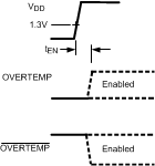 Figure 1. Definition of tEN
 Figure 2. Definition of tVTEMP
6.9 Typical Characteristics
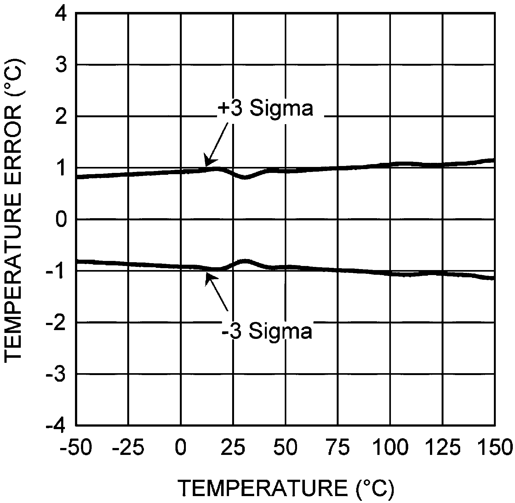 Figure 3. VTEMP Output Temperature Error vs Temperature
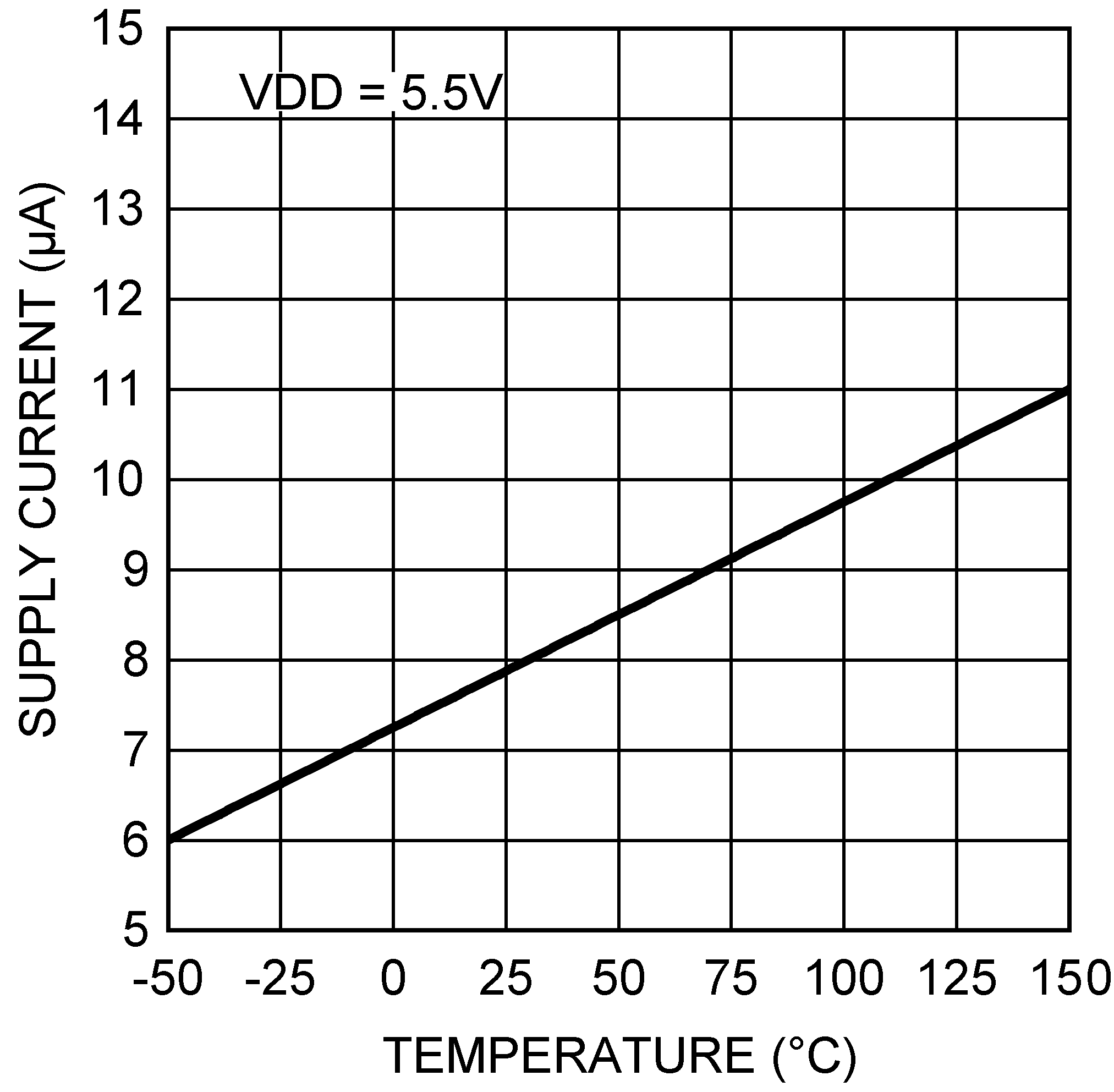 Figure 5. Supply Current vs Temperature
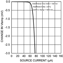
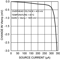
| 100-mV overhead | TA = 80°C | Sourcing current |
(1)The curves shown represent typical performance under worst-case conditions. Performance improves with larger VTEMP, larger VDD, and lower temperatures.
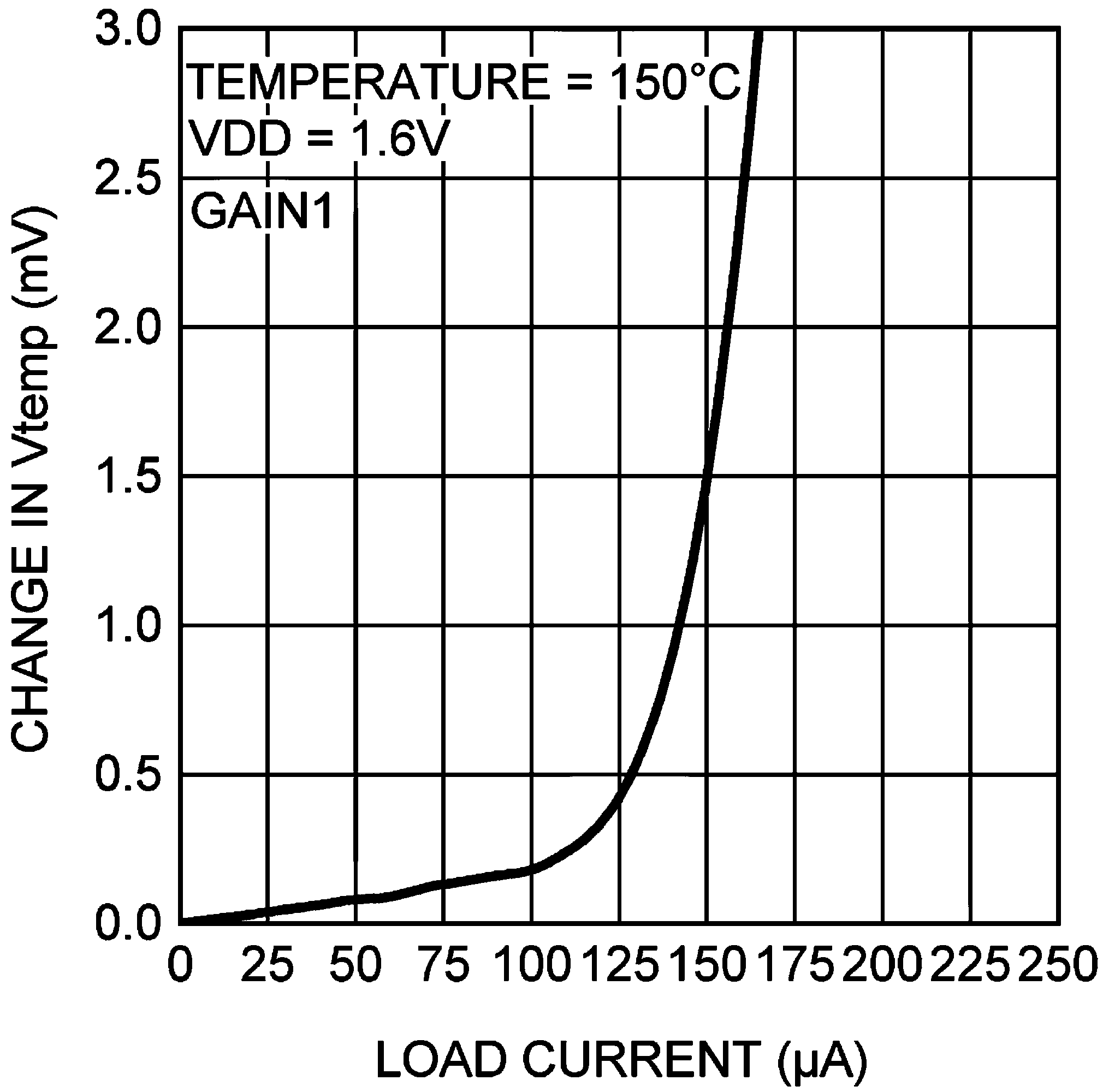
| VDD = 1.6 V | Sinking Current |
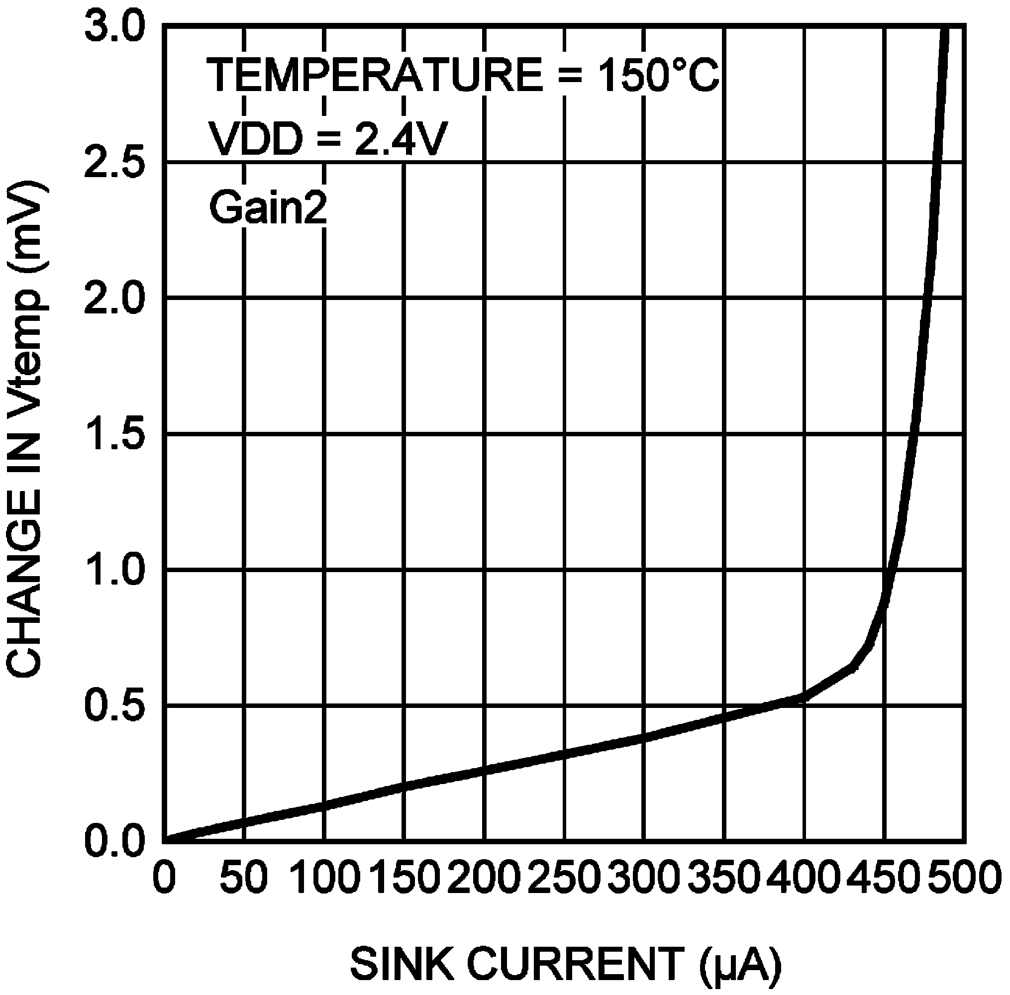
| VDD = 2.4 V | Sinking Current |
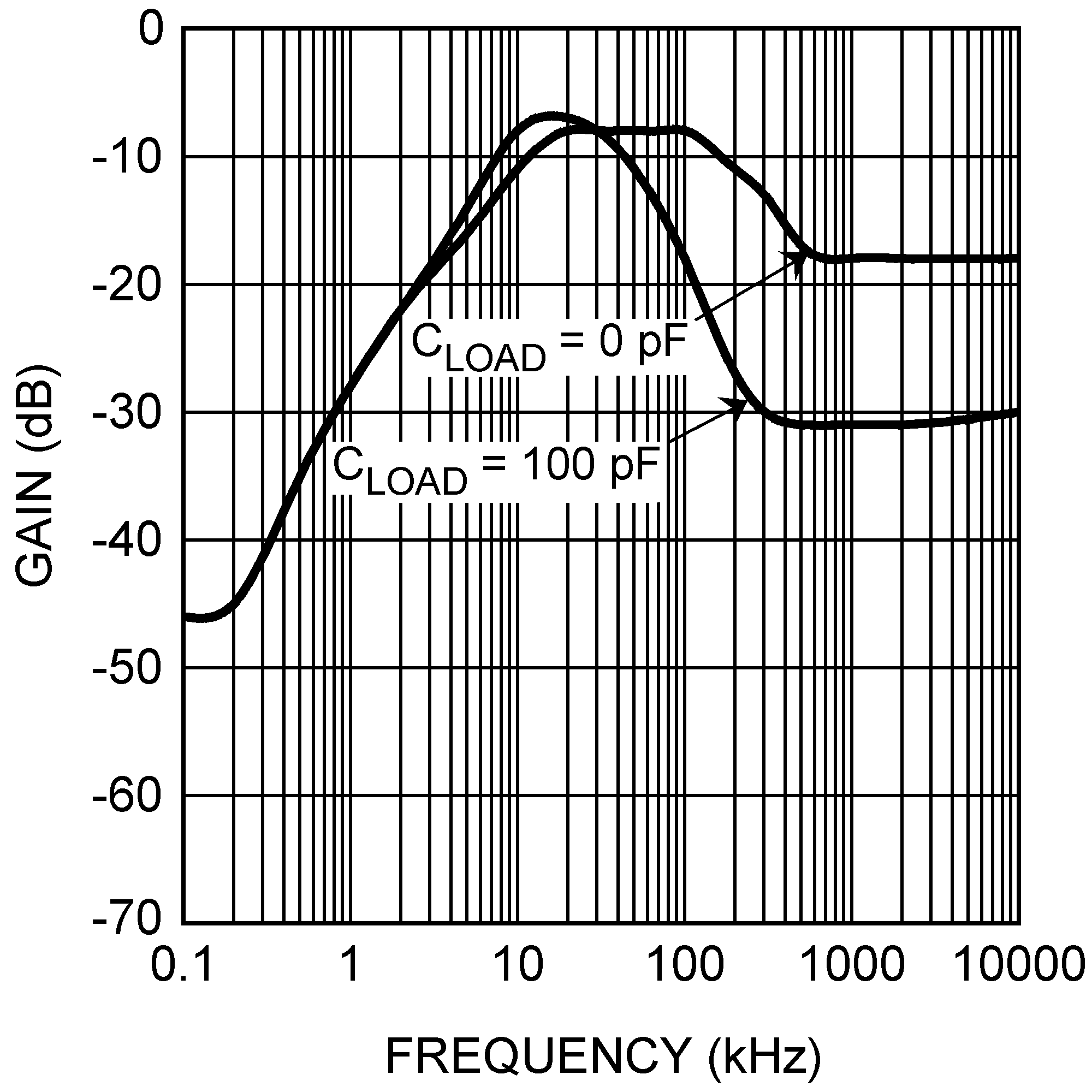
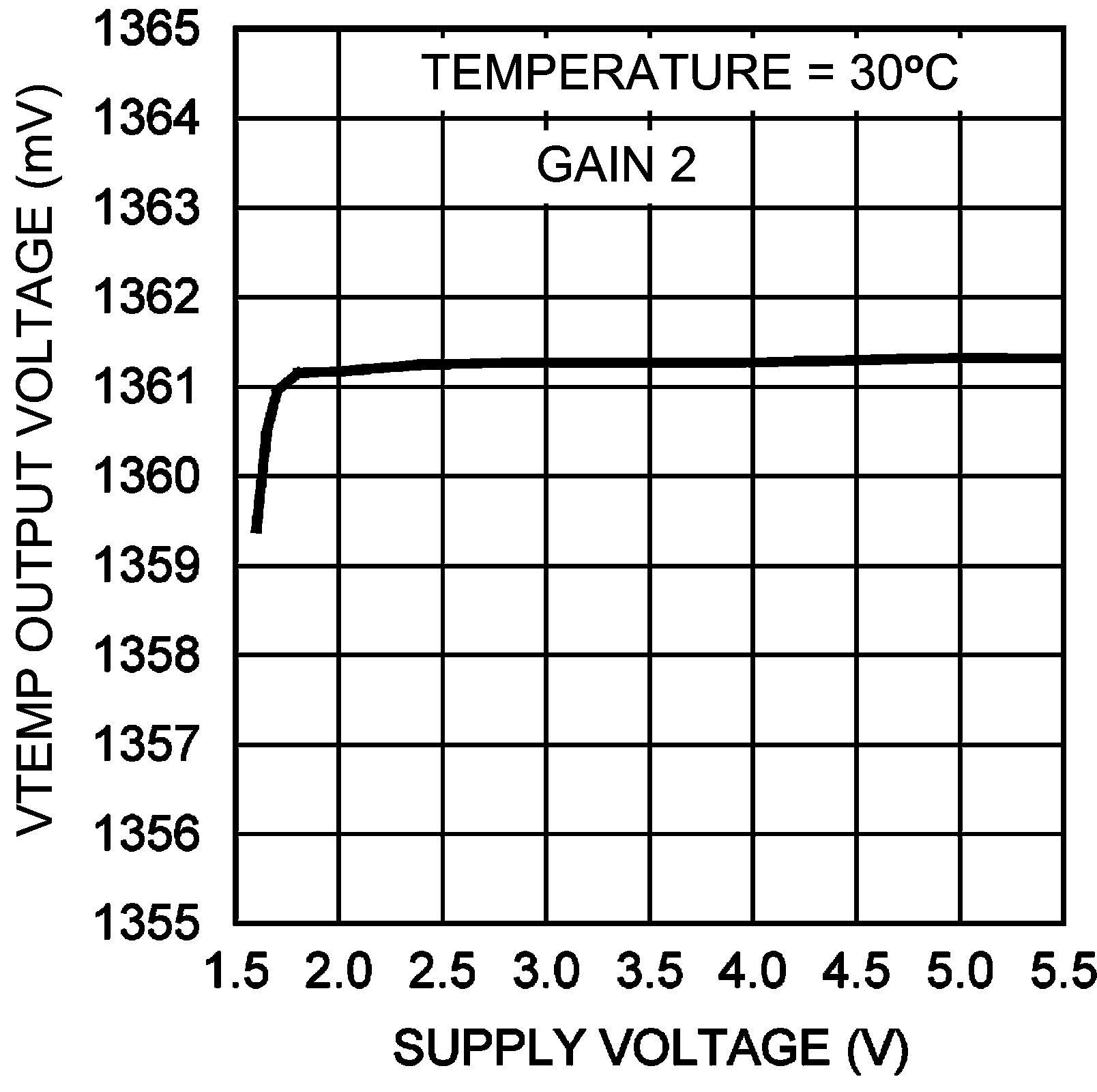
| Gain 2 (Trip Points = 70°C to 109°C) | ||
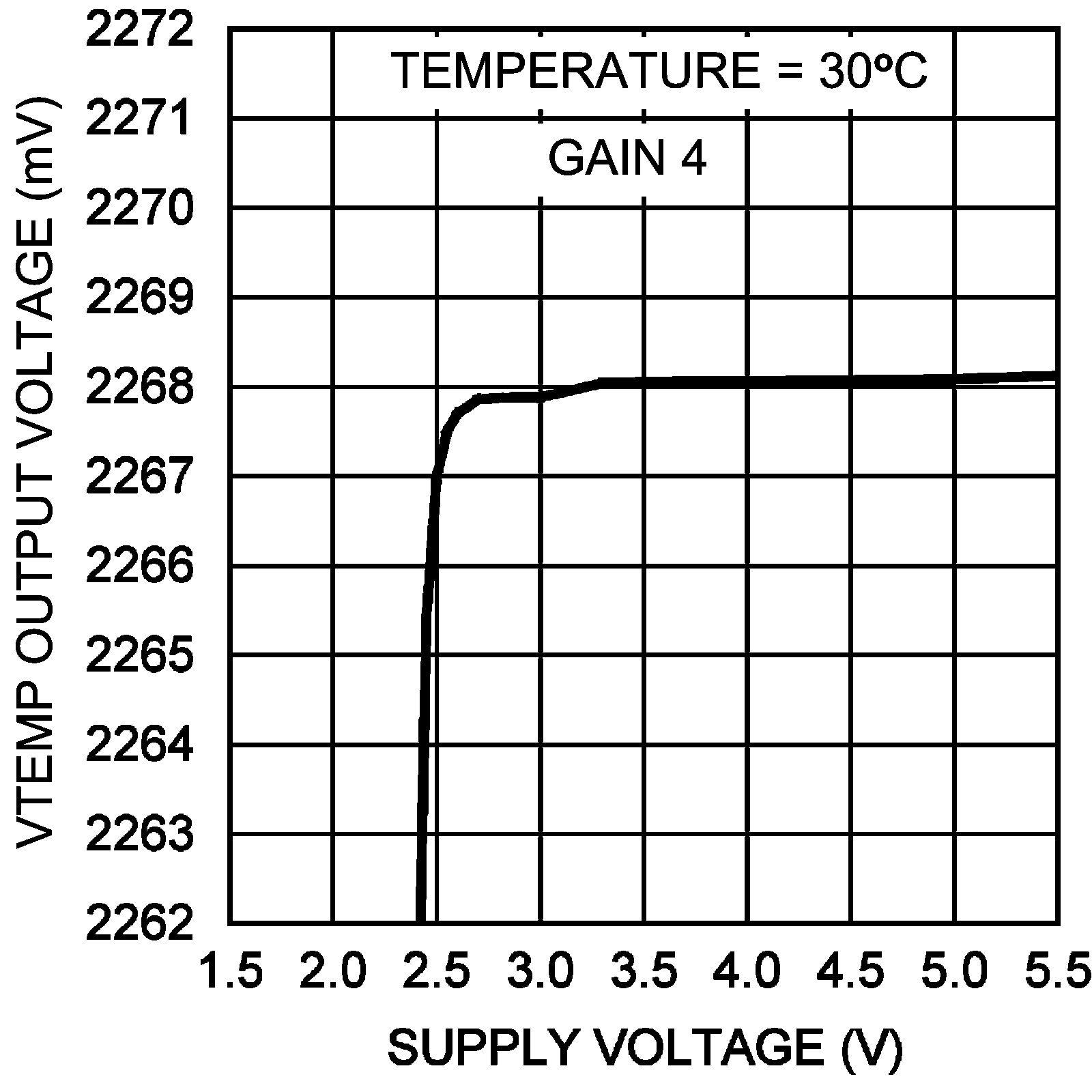
| Gain 4 (Trip Points = 130°C to 150°C) | ||
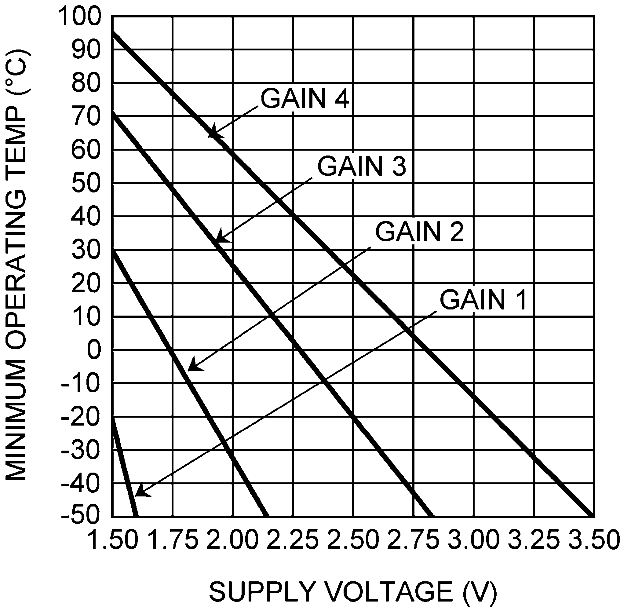 Figure 4. Minimum Operating Temperature
vs Supply Voltage
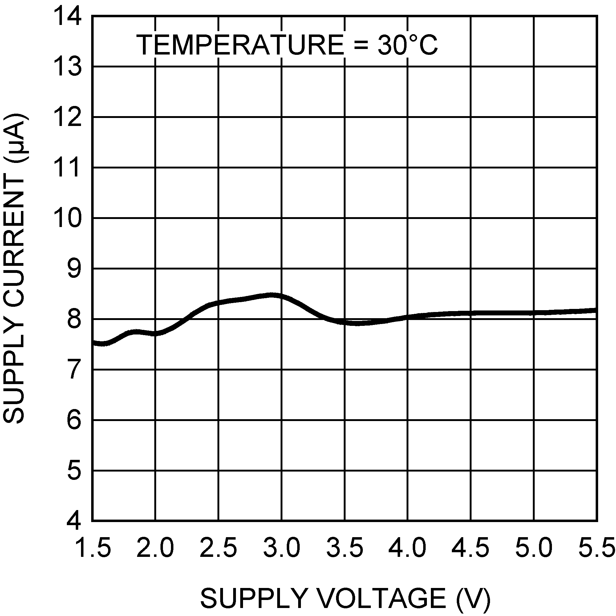 Figure 6. Supply Current vs Supply Voltage
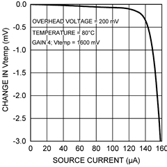
| 200-mV overhead | TA = 80°C | Sourcing Current |
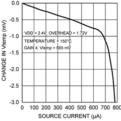
| 1.72-V overhead TA = 150°C | VDD = 2.4 V Sourcing current |
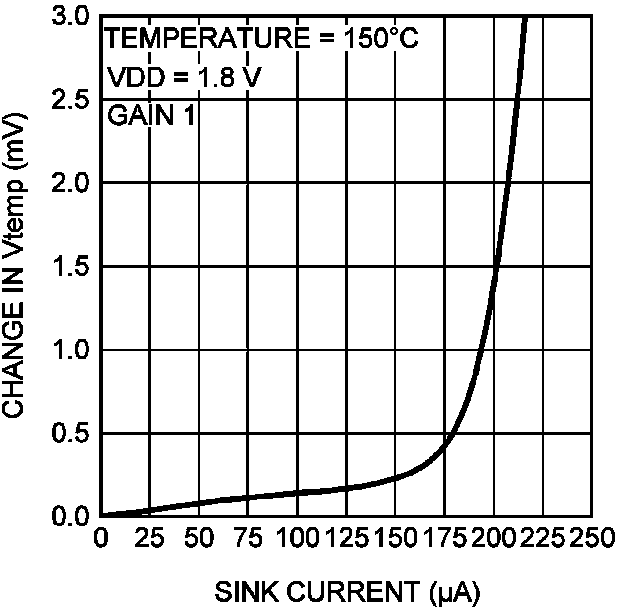
| VDD = 1.8 V | Sinking Current |
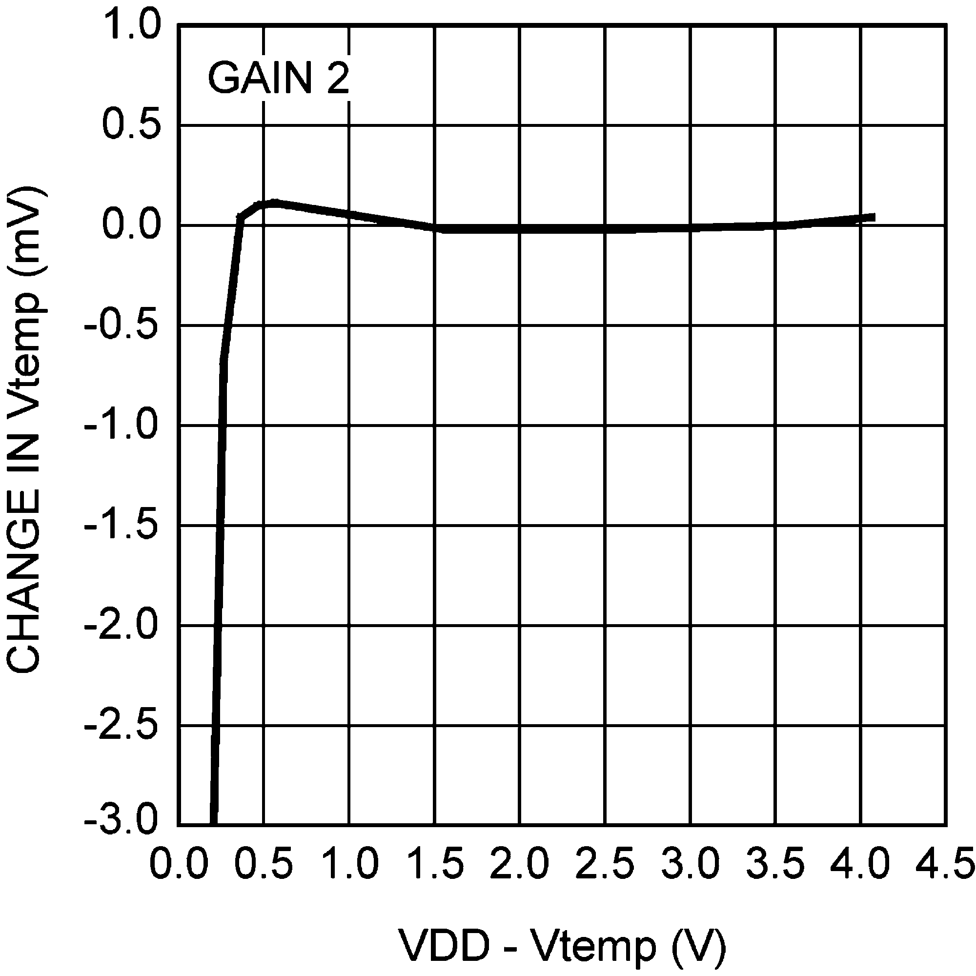
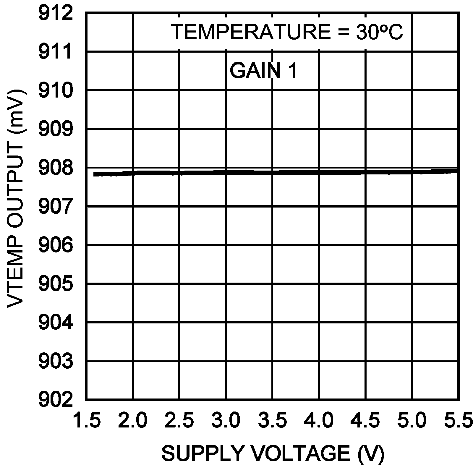
| Gain 1 (Trip Points = 0°C tp 69°C) | ||
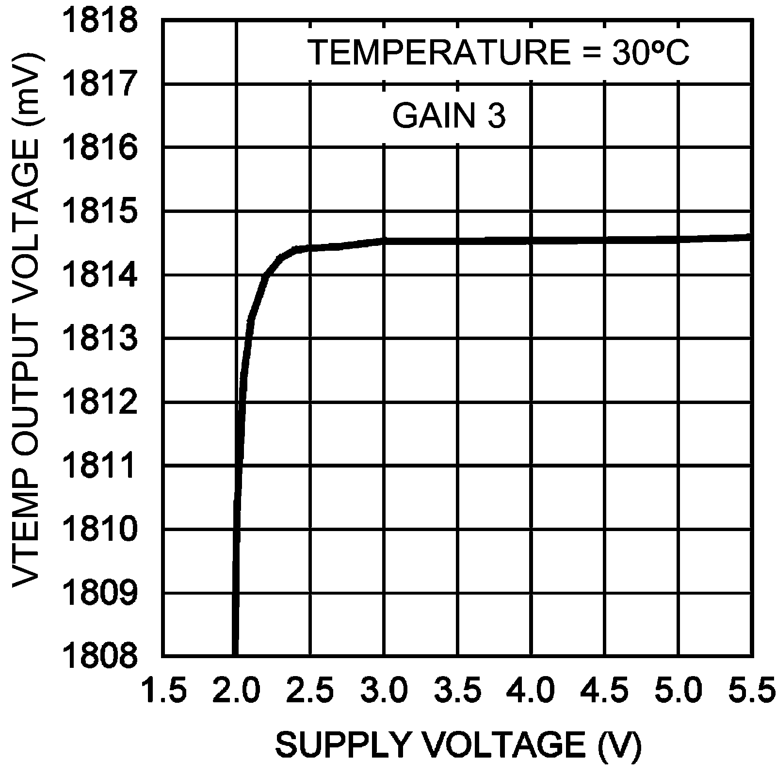
| Gain 3 (Trip Points = 110°C to 129°C) | ||
