SNVS497F November 2008 – September 2016 LM27341 , LM27341-Q1 , LM27342 , LM27342-Q1
PRODUCTION DATA.
- 1 Features
- 2 Applications
- 3 Description
- 4 Revision History
- 5 Pin Configuration and Functions
- 6 Specifications
- 7 Detailed Description
-
8 Application and Implementation
- 8.1
Application Information
- 8.1.1 Inductor Selection
- 8.1.2 Inductor Material Selection
- 8.1.3 Input Capacitor
- 8.1.4 Output Capacitor
- 8.1.5 Catch Diode
- 8.1.6 Boost Diode (Optional)
- 8.1.7 Boost Capacitor
- 8.1.8 Output Voltage
- 8.1.9 Feedforward Capacitor (Optional)
- 8.1.10
Calculating Efficiency and Junction Temperature
- 8.1.10.1 Schottky Diode Conduction Losses
- 8.1.10.2 Inductor Conduction Losses
- 8.1.10.3 MOSFET Conduction Losses
- 8.1.10.4 MOSFET Switching Losses
- 8.1.10.5 IC Quiescent Losses
- 8.1.10.6 MOSFET Driver Losses
- 8.1.10.7 Total Power Losses
- 8.1.10.8 Efficiency Calculation Example
- 8.1.10.9 Calculating Junction Temperature
- 8.2
Typical Applications
- 8.2.1 LM2734x Configuration From VIN = 7 V to 16 V, VOUT = 5 V For Full Load at 2 MHz
- 8.2.2 LM2734x Configuration From VIN = 7 V to 16 V, VOUT = 5 V For Full Load at 1 MHz
- 8.2.3 LM2734x Configuration From VIN = 5 V to 16 V, VOUT = 3.3 V For Full Load at 2 MHz
- 8.2.4 LM2734x Configuration From VIN = 5 V to 16 V, VOUT = 3.3 V For Full Load at 2 MHz With SYNC = GND
- 8.2.5 LM2734x Configuration From VIN = 5 V to 16 V, VOUT = 3.3 V For Full Load at 2 MHz With SYNC = 1 MHz
- 8.2.6 LM2734x Configuration From VIN = 3.3 V to 16 V, VOUT = 1.8 V For Full Load at 2 MHz With SYNC = 1 GND
- 8.2.7 LM2734x Configuration From VIN = 3.3 V to 16 V, VOUT = 1.8 V For Full Load at 2 MHz With SYNC = 1 MHz
- 8.2.8 LM2734x Configuration From VIN = 3.3 V to 9 V, VOUT = 1.2 V For Full Load at 2 MHz With SYNC = 2 MHz
- 8.1
Application Information
- 9 Power Supply Recommendations
- 10Layout
- 11Device and Documentation Support
- 12Mechanical, Packaging, and Orderable Information
8 Application and Implementation
NOTE
Information in the following applications sections is not part of the TI component specification, and TI does not warrant its accuracy or completeness. TI’s customers are responsible for determining suitability of components for their purposes. Customers should validate and test their design implementation to confirm system functionality.
8.1 Application Information
8.1.1 Inductor Selection
Inductor selection is critical to the performance of the LM2734x and LM2734x-Q1. The selection of the inductor affects stability, transient response and efficiency. A key factor in inductor selection is determining the ripple current (ΔiL) (see Figure 27). The ripple current (ΔiL) is important in many ways.
First, by allowing more ripple current, lower inductance values can be used with a corresponding decrease in physical dimensions and improved transient response. On the other hand, allowing less ripple current increases the maximum achievable load current and reduce the output voltage ripple (see Output Capacitor for more details on calculating output voltage ripple). Increasing the maximum load current is achieved by ensuring that the peak inductor current (ILPK) never exceeds the minimum current limit of 2 A for the LM27341 or 2.5 A for the LM27342 in Equation 8.
Secondly, the slope of the ripple current affects the current control loop. The LM2734x and LM2734x-Q1 have a fixed slope corrective ramp. When the slope of the current ripple becomes significantly less than the converter’s corrective ramp, the inductor pole moves from high frequencies to lower frequencies. This negates one advantage that peak current-mode control has overvoltage-mode control, which is, a single low-frequency pole in the power stage of the converter. This can reduce the phase margin, crossover frequency and potentially cause instability in the converter. Contrarily, when the slope of the ripple current becomes significantly greater than the converter’s corrective ramp, resonant peaking can occur in the control loop. This can also cause instability (subharmonic oscillation) in the converter. For the power supply designer, this means that for lower switching frequencies the current ripple must be increased to keep the inductor pole well above crossover. It also means that for higher switching frequencies the current ripple must be decreased to avoid resonant peaking.
With all these factors, the desired ripple current is selected with Equation 9. The ripple ratio (r) is defined as the ratio of inductor ripple current (ΔiL) to output current (IOUT), evaluated at maximum load.

A good compromise between physical size, transient response and efficiency is achieved when we set the ripple ratio between 0.2 and 0.4. The recommended ripple ratio versus duty cycle shown in Figure 31 is based upon this compromise and control loop optimizations. Note that this is just a guideline. See AN-1197 Selecting Inductors for Buck Converters for further considerations.
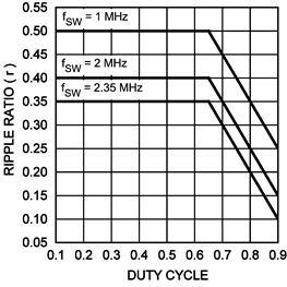 Figure 31. Recommended Ripple Ratio vs Duty Cycle
The duty cycle (D) can be approximated quickly using the ratio of output voltage (VOUT) to input voltage (VIN) in Equation 10.

The application's lowest input voltage must be used to calculate the ripple ratio. The catch diode forward voltage drop (VD1) and the voltage drop across the internal NFET (VDS) must be included to calculate a more accurate duty cycle. Calculate D by using Equation 11.

VDS can be approximated with Equation 12.
The diode forward drop (VD1) can range from 0.3 V to 0.5 V depending on the quality of the diode. The lower VD1 is, the higher the operating efficiency of the converter.
Now that the ripple current or ripple ratio is determined, the required inductance is calculated with Equation 13.

where
- DMIN is the duty cycle calculated with the maximum input voltage
- fsw is the switching frequency
- IOUT is the maximum output current of 2 A
Using IOUT = 2 A minimizes the inductor's physical size.
8.1.1.1 Inductor Calculation Example
Operating conditions for the LM27342 are listed in Table 1.
Table 1. Operating Conditions for Inductor Example
| OPERATING PARAMETERS | ||
|---|---|---|
| VIN = 7 – 16 V | VOUT = 3.3 V | IOUT = 2 A |
| fSW = 2 MHz | VD1 = 0.5 V | |
First the maximum duty cycle is calculated with Equation 14.
Using Figure 31 gives us a recommended ripple ratio = 0.4.
Now the minimum duty cycle is calculated with Equation 15.
The inductance can now be calculated with Equation 16.
This is close to the standard inductance value of 1.8 µH. This leads to a 1% deviation from the recommended ripple ratio, which is now 0.4038.
Finally, we check that the peak current does not reach the minimum current limit of 2.5 A with Equation 17.
The peak current is less than 2.5 A, so the DC load specification can be met with this ripple ratio. To design for the LM27341 simply replace IOUT = 1.5 A in the equations for ILPK and see that ILPK does not exceed the LM27341's current limit of 2 A (minimum).
8.1.2 Inductor Material Selection
When selecting an inductor, make sure that it is capable of supporting the peak output current without saturating. Inductor saturation results in a sudden reduction in inductance and prevent the regulator from operating correctly. To prevent the inductor from saturating over the entire –40 °C to 125 °C range, pick an inductor with a saturation current higher than the upper limit of ICL listed in Electrical Characteristics.
Ferrite core inductors are recommended to reduce AC loss and fringing magnetic flux. The drawback of ferrite core inductors is their quick saturation characteristic. The current limit circuit has a propagation delay and so is oftentimes not fast enough to stop a saturated inductor from going above the current limit. This has the potential to damage the internal switch. To prevent a ferrite core inductor from getting into saturation, the inductor saturation current rating must be higher than the switch current limit ICL. The LM2734x and LM2734x-Q1 are quite robust in handling short pulses of current that are a few amps above the current limit. Saturation protection is provided by a second current limit which is 30% higher than the cycle by cycle current limit. When the saturation protection is triggered the part turns off the output switch and attempt to soft start. When a compromise must be made, pick an inductor with a saturation current just above the lower limit of the ICL. Be sure to validate the short-circuit protection over the intended temperature range.
An inductor's saturation current is usually lower when hot. So consult the inductor vendor if the saturation current rating is only specified at room temperature.
Soft saturation inductors such as the iron powder types can also be used. Such inductors do not saturate suddenly and therefore are safer when there is a severe overload or even shorted output. Their physical sizes are usually smaller than the Ferrite core inductors. The downside is their fringing flux and higher power dissipation due to relatively high AC loss, especially at high frequencies.
8.1.3 Input Capacitor
An input capacitor is necessary to ensure that VIN does not drop excessively during switching transients. The primary specifications of the input capacitor are capacitance, voltage, RMS current rating, and Equivalent Series Inductance (ESL). The recommended input capacitance is 10 µF, although 4.7 µF works well for input voltages below 6 V. The input voltage rating is specifically stated by the capacitor manufacturer. Make sure to check any recommended deratings and also verify if there is any significant change in capacitance at the operating input voltage and the operating temperature. The input capacitor maximum RMS input current rating (IRMS-IN) must be greater than Equation 18.

where
- r is the ripple ratio defined earlier
- IOUT is the output current
- D is the duty cycle
Equation 18 shows that maximum RMS capacitor current occurs when D = 0.5. Always calculate the RMS at the point where the duty cycle, D, is closest to 0.5. The ESL of an input capacitor is usually determined by the effective cross sectional area of the current path. A large leaded capacitor has high ESL and a 0805 ceramic chip capacitor has very low ESL. At the operating frequencies of the LM2734x and LM2734x-Q1, certain capacitors may have an ESL so large that the resulting impedance (2πfL) is higher than that required to provide stable operation. As a result, TI strongly recommends surface-mount capacitors. Sanyo POSCAP, Tantalum or Niobium, Panasonic SP or Cornell Dubilier Low ESR are all good choices for input capacitors and have acceptable ESL. Multilayer ceramic capacitors (MLCC) have very low ESL. For MLCCs, TI recommends using X7R or X5R dielectrics. Consult the capacitor manufacturer's data sheet to see how rated capacitance varies over operating conditions.
8.1.4 Output Capacitor
The output capacitor is selected based upon the desired output ripple and transient response. The LM2734x and LM2734x-Q1 loop compensation is designed for ceramic capacitors. A minimum of 22 µF is required at 2 MHz
(33 µF at 1 MHz) while 47 µF to 100 µF is recommended for improved transient response and higher phase margin. The output voltage ripple of the converter is calculated with Equation 19.

When using MLCCs, the ESR is typically so low that the capacitive ripple may dominate. When this occurs, the output ripple is approximately sinusoidal and 90° phase shifted from the switching action. Another benefit of ceramic capacitors is their ability to bypass high-frequency noise. A certain amount of switching edge noise couples through parasitic capacitances in the inductor to the output. A ceramic capacitor bypasses this noise while a tantalum does not.
The transient response is determined by the speed of the control loop and the ability of the output capacitor to provide the initial current of a load transient. Capacitance can be increased significantly with little detriment to the regulator stability. However, increasing the capacitance provides dimininshing improvement over 100 µF in most applications, because the bandwidth of the control loop decreases as output capacitance increases. If improved transient performance is required, add a feedforward capacitor. This becomes especially important for higher output voltages where the bandwidth of the LM2734x and LM2734x-Q1 is lower (see Feedforward Capacitor (Optional) and Frequency Synchronization for more information).
Check the RMS current rating of the capacitor. The RMS current rating of the capacitor chosen must also meet the following condition with Equation 20.

where
- IOUT is the output current
- r is the ripple ratio
8.1.5 Catch Diode
The catch diode (D1) conducts during the switch off-time. A Schottky diode is recommended for its fast switching times and low forward voltage drop. The catch diode must be chosen so that its current rating is greater than Equation 21.
The reverse breakdown rating of the diode must be at least the maximum input voltage plus appropriate margin. To improve efficiency, choose a Schottky diode with a low forward voltage drop.
8.1.6 Boost Diode (Optional)
For circuits with input voltages VIN < 5 V and duty cycles (D) > 0.75 V, TI recommends a small-signal Schottky diode. A good choice is the BAT54 small signal diode. The cathode of the diode is connected to the BOOST pin and the anode to a 5-V voltage rail.
8.1.7 Boost Capacitor
A ceramic 0.1-µF capacitor with a voltage rating of at least 6.3 V is sufficient. The X7R and X5R MLCCs provide the best performance.
8.1.8 Output Voltage
The output voltage is set using the following equation where R2 is connected between the FB pin and GND, and R1 is connected between VOUT and the FB pin in Equation 22. A good starting value for R2 is 1 kΩ.

8.1.9 Feedforward Capacitor (Optional)
A feedforward capacitor (CFF) can improve the transient response of the converter. Place CFF in parallel with R1. The value of CFF must place a zero in the loop response at, or above, the pole of the output capacitor and RLOAD as calculated in Equation 23. The CFF capacitor increases the crossover frequency of the design, thus a larger minimum output capacitance is required for designs using CFF. CFF must only be used with an output capacitance greater than or equal to 44 µF.

8.1.10 Calculating Efficiency and Junction Temperature
The complete LM2734x and LM2734x-Q1 DC-DC converter efficiency can be calculated with Equation 24 or Equation 25.


To determine the most significant power losses, see the following equations. Other losses totaling less than 2% are not discussed.
Power loss (PLOSS) is the sum of two basic types of losses in the converter, switching and conduction. Conduction losses usually dominate at higher output loads, where as switching losses remain relatively fixed and dominate at lower output loads. The first step in determining the losses is to calculate the duty cycle (D) with Equation 26.

VDS is the voltage drop across the internal NFET when it is on, and is equal to Equation 27.
VD is the forward voltage drop across the Schottky diode. It can be obtained from the Electrical Characteristics section of the Schottky diode data sheet. If the voltage drop across the inductor (VDCR) is accounted for, the equation changes to Equation 28.

VDCR usually gives only a minor duty cycle change, and has been omitted in the examples for simplicity.
8.1.10.1 Schottky Diode Conduction Losses
The conduction losses in the free-wheeling Schottky diode are calculated with Equation 29.
Often this is the single most significant power loss in the circuit. Care must be taken to choose a Schottky diode that has a low forward voltage drop.
8.1.10.2 Inductor Conduction Losses
Another significant external power loss is the conduction loss in the output inductor. The equation can be simplified to Equation 30.
8.1.10.3 MOSFET Conduction Losses
The LM2734x and LM2734x-Q1 conduction loss is mainly associated with the internal NFET calculated with Equation 31.
8.1.10.4 MOSFET Switching Losses
Switching losses are also associated with the internal NFET. They occur during the switch on and off transition periods, where voltages and currents overlap resulting in power loss. The simplest means to determine this loss is to empirically measuring the rise and fall times (10% to 90%) of the switch at the switch node with Equation 32, Equation 33, and Equation 34. Typical values are listed in Table 2.
Table 2. Typical Rise and Fall Times vs Input Voltage
| VIN | tRISE | tFALL |
|---|---|---|
| 5 V | 8 ns | 8 ns |
| 10 V | 9 ns | 9 ns |
| 15 V | 10 ns | 10 ns |
8.1.10.5 IC Quiescent Losses
Another loss is the power required for operation of the internal circuitry calculated with Equation 35.
IQ is the quiescent operating current, and is typically around 2.4 mA.
8.1.10.6 MOSFET Driver Losses
The other operating power that needs calculation is that required to drive the internal NFET with Equation 36.
VBOOST is normally between 3 VDC and 5 VDC. The IBOOST rms current is dependant on switching frequency fSW. IBOOST is approximately 8.2 mA at 2 MHz and 4.4 mA at 1 MHz.
8.1.10.7 Total Power Losses
Total power losses is calculated with Equation 37.
Losses internal to the LM2734x and LM2734x-Q1 is calculated with Equation 38.
8.1.10.8 Efficiency Calculation Example
Operating conditions are listed in Table 3.
Table 3. Operating Conditions for Efficiency Calculation
| OPERATING PARAMETERS | ||
|---|---|---|
| VIN = 12 V | VOUT = 3.3 V | IOUT = 2 A |
| fSW = 2 MHZ | VD1 = 0.5 V | RDCR = 20 mΩ |
Internal power losses are calculated with Equation 39 through Equation 43.
Total power losses are calculated with Equation 44 through Equation 46.
The efficiency can now be estimated with Equation 47.

With this information, we can estimate the junction temperature of the LM2734x and LM2734x-Q1.
8.1.10.9 Calculating Junction Temperature
The thermal definitions are:
- TJ = IC junction temperature
- TA = Ambient temperature
- RθJC = Thermal resistance from IC junction to device case
- RθJA = Thermal resistance from IC junction to ambient air
 Figure 32. Cross-Sectional View of Integrated Circuit Mounted on a Printed Circuit Board
Heat in the LM2734x and LM2734x-Q1 due to internal power dissipation is removed through conduction and/or convection.
8.1.10.9.1 Conduction
Heat transfer occurs through cross sectional areas of material. Depending on the material, the transfer of heat can be considered to have poor-to-good thermal conductivity properties (insulator versus conductor).
Heat transfer goes from Silicon → Lead Frame → PCB.
8.1.10.9.2 Convection
Heat transfer is by means of airflow. This could be from a fan or natural convection. Natural convection occurs when air currents rise from the hot device to cooler air.
Thermal impedance is defined with Equation 48.

Thermal impedance from the silicon junction to the ambient air is defined with Equation 49.

This impedance can vary depending on the thermal properties of the PCB. This includes PCB size, weight of copper used to route traces , the ground plane, and the number of layers within the PCB. The type and number of thermal vias can also make a large difference in the thermal impedance. Thermal vias are necessary in most applications. They conduct heat from the surface of the PCB to the ground plane. Six to nine thermal vias must be placed under the exposed pad to the ground plane. Placing more than nine thermal vias results in only a small reduction to RθJA for the same copper area. These vias must have 8-mil holes to avoid wicking solder away from the DAP. See AN-1187 Leadless Leadframe Package (SNOA401) and AN-1520 A Guide to Board Layout for Best Thermal Resistance for Exposed Packages (SNVA183) for more information on package thermal performance. If a compromise for cost needs to be made, the thermal vias for the MSOP-PowerPAD package can range from 8 mils to 14 mils, increasing the possibility of solder wicking.
To predict the silicon junction temperature for a given application, three methods can be used. The first is useful before prototyping and the other two can more accurately predict the junction temperature within the application.
8.1.10.9.3 Method 1
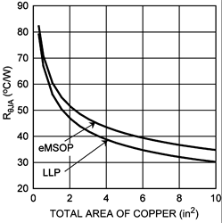
The first method predicts the junction temperature by extrapolating a best guess RθJA from the table or graph. The tables and graph are for natural convection. The internal dissipation can be calculated using the efficiency calculations. This allows the user to make a rough prediction of the junction temperature in their application. Methods two and three can later be used to determine the junction temperature more accurately.
Table 4 and Table 5 have values of RθJA for the WSON and the MSOP-PowerPAD packages.
Table 4. RθJA Values for the MSOP-PowerPAD at 1-W Dissipation
| NUMBER OF BOARD LAYERS | SIZE OF BOTTOM LAYER COPPER CONNECTED TO DAP | SIZE OF TOP LAYER COPPER CONNECTED TO DAP | NUMBER OF 10 MIL THERMAL VIAS | RθJA |
| 2 | 0.25 in2 | 0.05 in2 | 8 | 80.6°C/W |
| 2 | 0.5625 in2 | 0.05 in2 | 8 | 70.9°C/W |
| 2 | 1 in2 | 0.05 in2 | 8 | 62.1°C/W |
| 2 | 1.3225 in2 | 0.05 in2 | 8 | 54.6°C/W |
| 4 (eval board) | 3.25 in2 | 2.25 in2 | 14 | 35.3°C/W |
Table 5. RθJA Values for the WSON at 1-W Dissipation
| NUMBER OF BOARD LAYERS | SIZE OF BOTTOM LAYER COPPER CONNECTED TO DAP | SIZE OF TOP LAYER COPPER CONNECTED TO DAP | NUMBER OF 8 MIL THERMAL VIAS | RθJA |
| 2 | 0.25 in2 | 0.05 in2 | 8 | 78°C/W |
| 2 | 0.5625 in2 | 0.05 in2 | 8 | 65.6°C/W |
| 2 | 1 in2 | 0.05 in2 | 8 | 58.6°C/W |
| 2 | 1.3225 in2 | 0.05 in2 | 8 | 50°C/W |
| 4 (eval board) | 3.25 in2 | 2.25 in2 | 15 | 30.7°C/W |
8.1.10.9.4 Method 2
The second method requires the user to know the thermal impedance of the silicon junction to case. RθJC is approximately 9.5°C/W for the MSOP-PowerPAD package or 9.1°C/W for the WSON. The case temperature must be measured on the bottom of the PCB at a thermal through directly under the DAP of the LM2734x and LM2734x-Q1. The solder resist must be removed from this area for temperature testing. The reading is more accurate if it is taken midway between pins 2 and 9, where the NMOS switch is placed. Knowing the internal dissipation from Method 1, calculate the case temperature (TC) with Equation 50 and Equation 51.

8.1.10.9.4.1 Method 2 Example
The operating conditions are the same as the previous efficiency calculation listed in Table 6.
Table 6. Operating Conditions for Efficiency Calculation
| OPERATING PARAMETERS | ||
|---|---|---|
| VIN = 12 V | VOUT = 3.3 V | IOUT = 2 A |
| fSW = 2 MHz | VD1 = 0.5 V | RDCR = 20 mΩ |
Internal power losses are calculated with Equation 52 through Equation 56.
The junction temperature can now be estimated with Equation 57.
A TI MSOP-PowerPAD evaluation board was used to determine the TJ of the LM2734x and LM2734x-Q1. The four layer PCB is constructed using FR4 with 2-oz copper traces. There is a ground plane on the internal layer directly beneath the device, and a ground plane on the bottom layer. The ground plane is accessed by fourteen 10-mil vias. The board measures 2 in × 2 in (50.8 mm × 50.8 mm). It was placed in a container with no airflow. The case temperature measured on this LM27342MY Demo Board was 48.7°C. Therefore, TJ is calculated with Equation 58 and Equation 59.
To keep the junction temperature below 125°C for this layout, the ambient temperature must stay below
94.33°C as in Equation 60, Equation 61, and Equation 62.
8.1.10.9.5 Method 3
The third method can also give a very accurate estimate of silicon junction temperature. The first step is to determine RθJA of the application. The LM2734x and LM2734x-Q1 has overtemperature protection circuitry. When the silicon temperature reaches 165°C, the device stops switching. The protection circuitry has a hysteresis of 15°C. Once the silicon temperature has decreased to approximately 150°C, the device starts switching again. Knowing this, the RθJA for any PCB can be characterized during the early stages of the design by raising the ambient temperature in the given application until the circuit enters thermal shutdown. If the SW-pin is monitored, it is obvious when the internal NFET stops switching indicating a junction temperature of 165°C. We can calculate the internal power dissipation from the above methods. All that is required for calculation is the estimate of RDSON at 165°C. The value is approximately 0.267 Ω. With this, the junction temperature, and the ambient temperature, RθJA, can be determined with Equation 63.

Once this is determined, the maximum ambient temperature allowed for a desired junction temperature can be found.
8.1.10.9.5.1 Method 3 Example
The operating conditions are the same as the previous efficiency calculation listed in Table 7.
Table 7. Operating Conditions for Efficiency Calculation
| OPERATING PARAMETERS | ||
|---|---|---|
| VIN = 12 V | VOUT = 3.3 V | IOUT = 2A |
| fSW = 2 MHz | VD1 = 0.5 V | RDCR = 20 mΩ |
Internal power losses are calculated with Equation 64 through Equation 68.
A TI MSOP-PowerPAD evaluation board was used to determine the RθJA of the board. The four-layer PCB is constructed using FR4 with 2oz copper traces. There is a ground plane on the internal layer directly beneath the device, and a ground plane on the bottom layer. The ground plane is accessed by fourteen 10-mil vias. The board measures 2 in × 2 in (50.8 mm × 50.8 mm). It was placed in an oven with no forced airflow.
The ambient temperature was raised to 132°C, and at that temperature, the device went into thermal shutdown. RθJA can be calculated with Equation 69.

To keep the junction temperature below 125°C for this layout, the ambient temperature must stay below 92°C as in Equation 70, Equation 71, and Equation 72.
This calculation of the maximum ambient temperature is only 2.3°C different from the calculation using method 2. The methods described above to find the junction temperature in the MSOP-PowerPAD package can also be used to calculate the junction temperature in the WSON package. The 10-pin WSON package has a
RθJC = 9.1°C/W, while RθJA can vary depending on the layout. RθJA can be calculated in the same manner as described in method 3.
8.2 Typical Applications
8.2.1 LM2734x Configuration From VIN = 7 V to 16 V, VOUT = 5 V For Full Load at 2 MHz
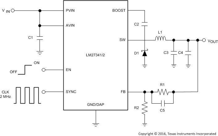
| VIN = 7 V to 16 V, VOUT = 5 V | fSW = 2 MHz | IOUT = Full load |
8.2.1.1 Design Requirements
Create 5-V output at full-rated load for VIN range of 7 V to 16 V with switching frequency FSW = 2 MHz using external synchronization.
8.2.1.2 Detailed Design Procedure
The device must be able to operate at any voltage within the recommended operating range. The load current must be defined to properly size the inductor, input, and output capacitors. The inductor must be able to handle the full expected load current as well as the peak current generated during load transients and start-up. The inrush current at start-up depends on the output capacitor selection.
Table 8 lists the bill of materials for VIN = 7 V to 16 V, VOUT = 5 V for full load at 2 MHz. See Figure 34.
Table 8. Bill of Materials
| PART NAME | PART ID | PART VALUE | PART NUMBER | MANUFACTURER |
|---|---|---|---|---|
| Buck regulator | U1 | 1.5-A or 2-A Buck regulator | LM2734x and LM2734x-Q1 | TI |
| CPVIN | C1 | 10 µF | GRM32DR71E106KA12L | Murata |
| CBOOST | C2 | 0.1 µF | GRM188R71C104KA01D | Murata |
| COUT | C3 | 22 µF | C3225X7R1C226K | TDK |
| COUT | C4 | 22 µF | C3225X7R1C226K | TDK |
| CFF | C5 | 0.18 µF | 0603ZC184KAT2A | AVX |
| Catch diode | D1 | Schottky diode, Vf = 0.32 V | CMS06 | Toshiba |
| Inductor | L1 | 2.2 µH | CDRHD5D28RHPNP | Sumida |
| Feedback resistor | R1 | 560 Ω | CRCW0603560RFKEA | Vishay |
| Feedback resistor | R2 | 140 Ω | CRCW0603140RFKEA | Vishay |
8.2.1.3 Application Curves
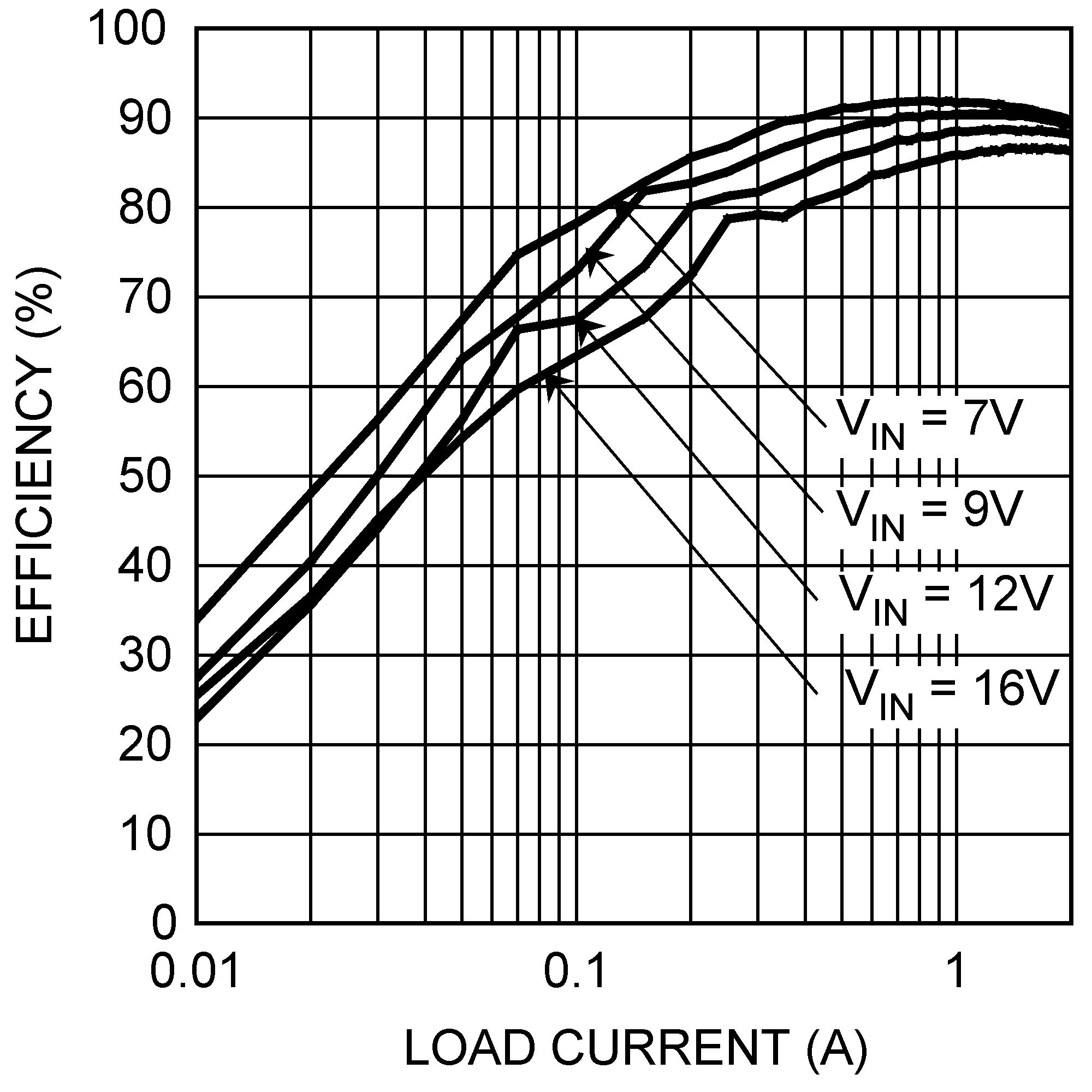 Figure 35. LM27342 Efficiency vs Load Current
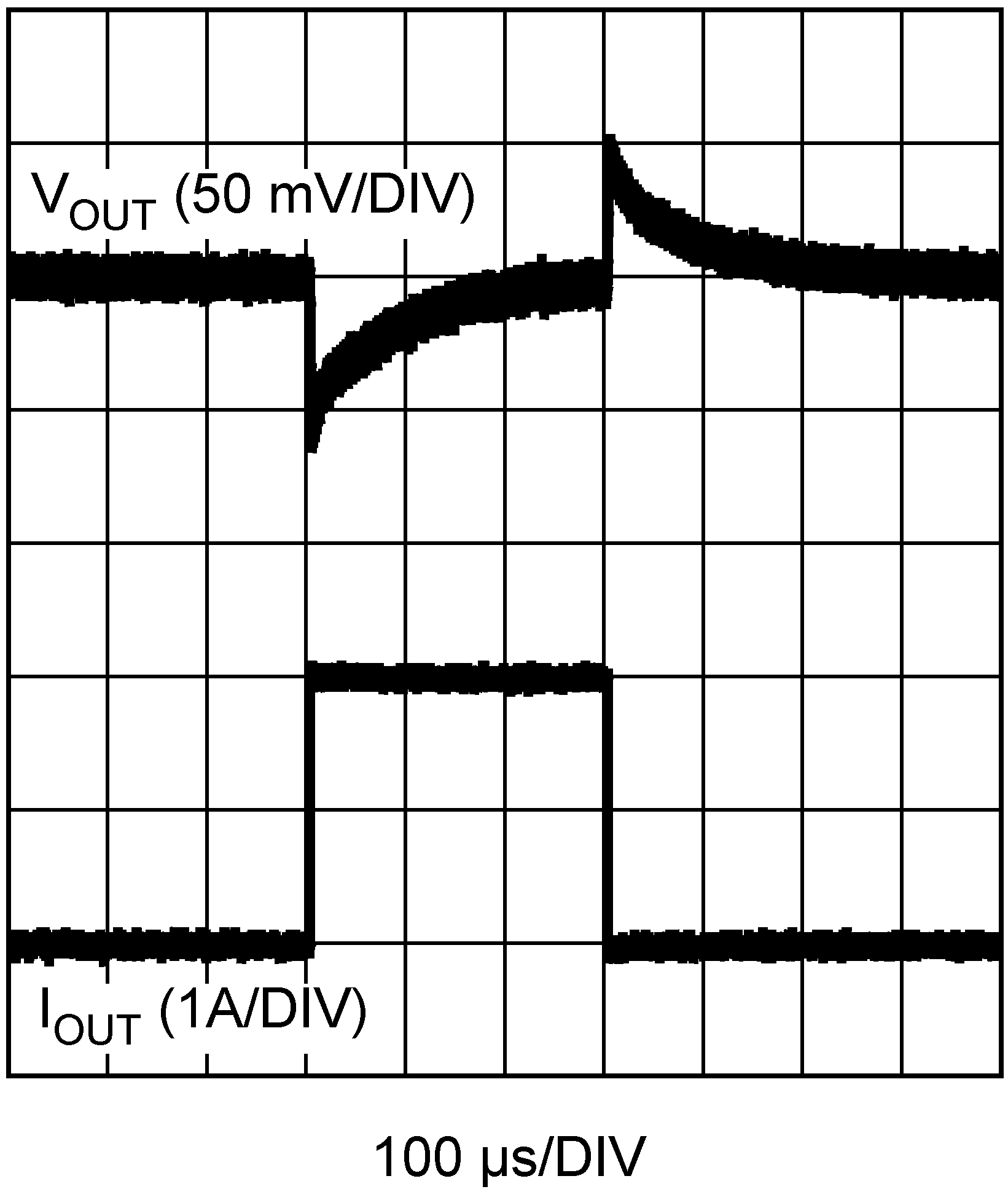
8.2.2 LM2734x Configuration From VIN = 7 V to 16 V, VOUT = 5 V For Full Load at 1 MHz
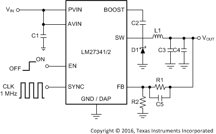
| VIN = 7 V to 16 V, VOUT = 5 V | fSW = 1 MHz | IOUT = Full load |
8.2.2.1 Design Requirements
Create 5-V output at full-rated load for VIN range of 7 V to 16 V with switching frequency FSW = 1 MHz using external synchronization.
8.2.2.2 Detailed Design Procedure
The device must be able to operate at any voltage within the recommended operating range. The load current must be defined to properly size the inductor, input, and output capacitors. The inductor must be able to handle the full expected load current as well as the peak current generated during load transients and start-up. The inrush current at start-up depends on the output capacitor selection.
Table 9 lists the bill of materials for VIN = 7 V to 16 V, VOUT = 5 V for full load at 1 MHz. See Figure 37.
Table 9. Bill of Materials
| PART NAME | PART ID | PART VALUE | PART NUMBER | MANUFACTURER |
|---|---|---|---|---|
| Buck regulator | U1 | 1.5-A or 2-A Buck regulator | LM2734x and LM2734x-Q1 | TI |
| CPVIN | C1 | 10 µF | GRM32DR71E106KA12L | Murata |
| CBOOST | C2 | 0.1 µF | GRM188R71C104KA01D | Murata |
| COUT | C3 | 47 µF | GRM32ER61A476KE20L | Murata |
| COUT | C4 | 22 µF | C3225X7R1C226K | TDK |
| CFF | C5 | 0.27 µF | C0603C274K4RACTU | Kemet |
| Catch diode | D1 | Schottky diode, Vf = 0.32 V | CMS06 | Toshiba |
| Inductor | L1 | 3.3 µH | CDRH6D26HPNP | Sumida |
| Feedback resistor | R1 | 560 Ω | CRCW0603560RFKEA | Vishay |
| Feedback resistor | R2 | 140 Ω | CRCW0603140RFKEA | Vishay |
8.2.2.3 Application Curves
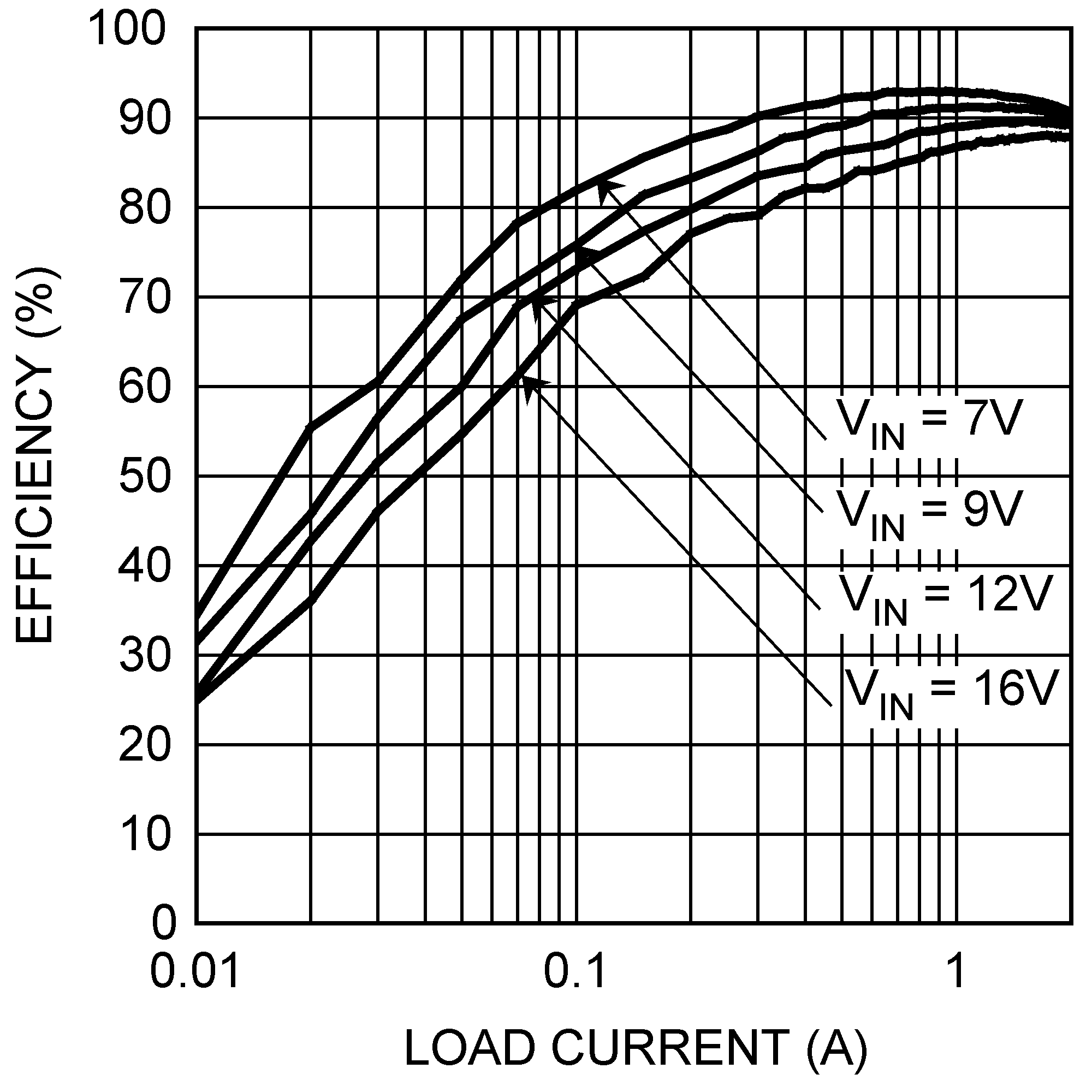 Figure 38. LM27342 Efficiency vs Load Current
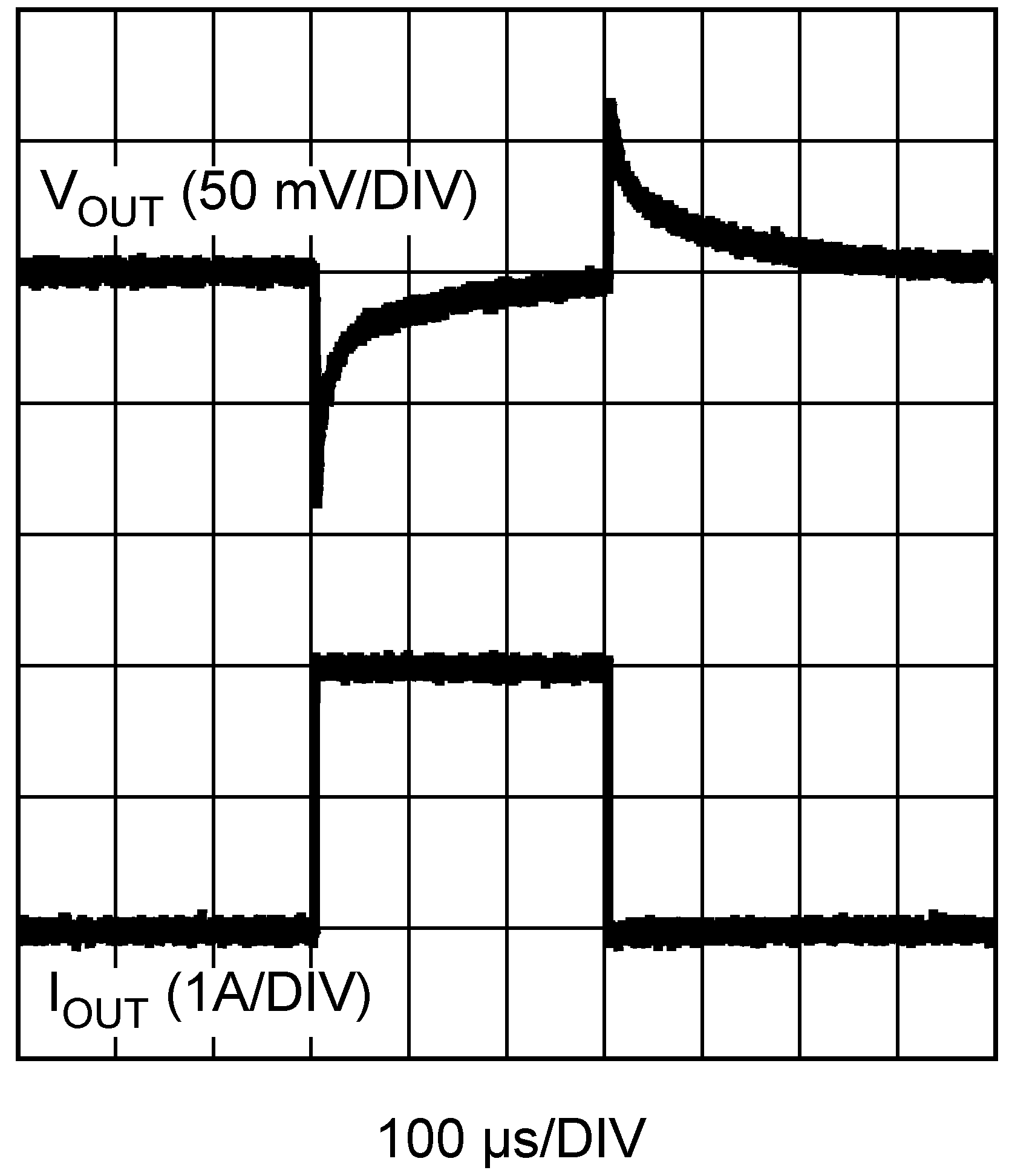
8.2.3 LM2734x Configuration From VIN = 5 V to 16 V, VOUT = 3.3 V For Full Load at 2 MHz

| VIN = 5 V to 16 V, VOUT = 3.3 V | fSW = 2 MHz | IOUT = Full load |
8.2.3.1 Design Requirements
Create 3.3-V output at full-rated load for VIN range of 5 V to 16 V with switching frequency FSW = 2 MHz using external synchronization.
8.2.3.2 Detailed Design Procedure
The device must be able to operate at any voltage within the recommended operating range. The load current must be defined to properly size the inductor, input, and output capacitors. The inductor must be able to handle the full expected load current as well as the peak current generated during load transients and start-up. The inrush current at start-up depends on the output capacitor selection.
Table 10 lists the bill of materials for VIN = 5 V to 16 V, VOUT = 3.3 V for full load at 2 MHz. See Figure 40.
Table 10. Bill of Materials
| PART NAME | PART ID | PART VALUE | PART NUMBER | MANUFACTURER |
|---|---|---|---|---|
| Buck regulator | U1 | 1.5-A or 2-A Buck regulator | LM2734x and LM2734x-Q1 | TI |
| CPVIN | C1 | 10 µF | GRM32DR71E106KA12L | Murata |
| CBOOST | C2 | 0.1 µF | GRM188R71C104KA01D | Murata |
| COUT | C3 | 22 µF | C3225X7R1C226K | TDK |
| COUT | C4 | 22 µF | C3225X7R1C226K | TDK |
| CFF | C5 | 0.18 µF | 0603ZC184KAT2A | AVX |
| Catch diode | D1 | Schottky diode, Vf = 0.32 V | CMS06 | Toshiba |
| Inductor | L1 | 1.5 µH | CDRH5D18BHPNP | Sumida |
| Feedback resistor | R1 | 430 Ω | CRCW0603430RFKEA | Vishay |
| Feedback resistor | R2 | 187 Ω | CRCW0603187RFKEA | Vishay |
8.2.3.3 Application Curves
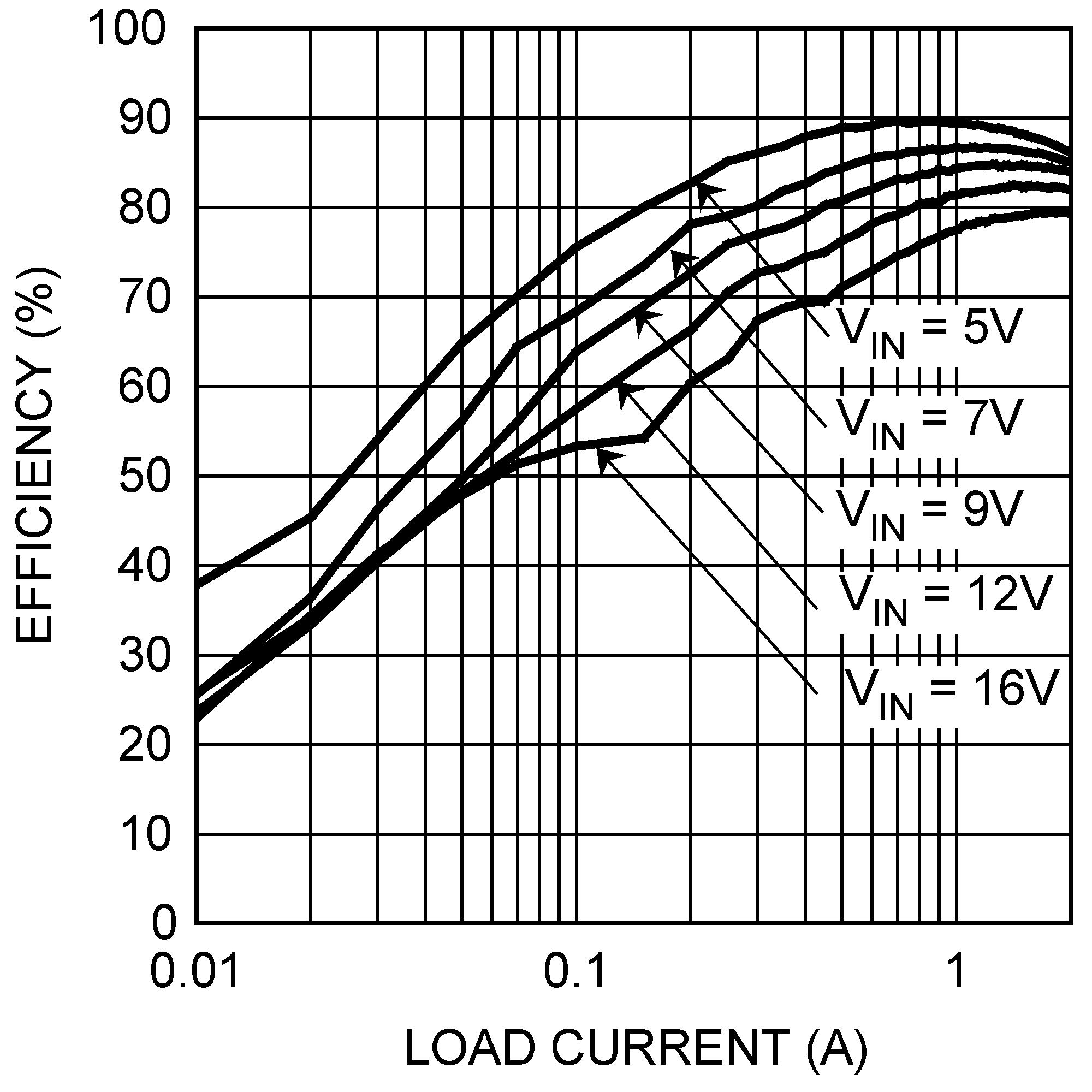 Figure 41. LM27342 Efficiency vs Load Current
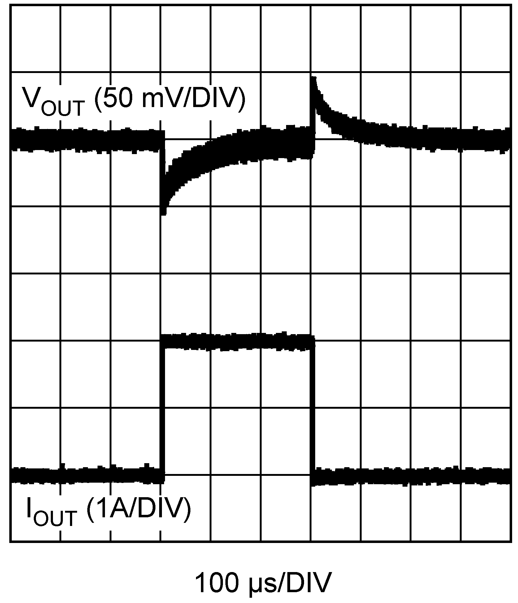
8.2.4 LM2734x Configuration From VIN = 5 V to 16 V, VOUT = 3.3 V For Full Load at 2 MHz
With SYNC = GND
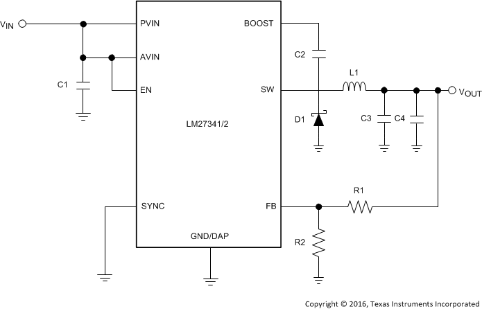
| VIN = 5 V to 16 V, VOUT = 3.3 V | fSW = 2 MHz | IOUT = Full load |
For Full Load at 2 MHz With SYNC = GND Schematic
8.2.4.1 Design Requirements
Create 3.3-V output at full-rated load for VIN range of 5 V to 16 V with switching frequency FSW = 2 MHz using internal oscillator.
8.2.4.2 Detailed Design Procedure
The device must be able to operate at any voltage within the recommended operating range. The load current must be defined to properly size the inductor, input, and output capacitors. The inductor must be able to handle the full expected load current as well as the peak current generated during load transients and start-up. The inrush current at start-up depends on the output capacitor selection.
Table 11 lists the bill of materials for VIN = 5 V to 16 V, VOUT = 3.3 V for full load at 2 MHz with SYNC = GND. See Figure 43.
Table 11. Bill of Materials
| PART NAME | PART ID | PART VALUE | PART NUMBER | MANUFACTURER |
|---|---|---|---|---|
| Buck regulator | U1 | 1.5-A or 2-A Buck regulator | LM2734x and LM2734x-Q1 | TI |
| CPVIN | C1 | 10 µF | GRM32DR71E106KA12L | Murata |
| CBOOST | C2 | 0.1 µF | GRM188R71C104KA01D | Murata |
| COUT | C3 | 22 µF | C3225X7R1C226K | TDK |
| COUT | C4 | 22 µF | C3225X7R1C226K | TDK |
| Catch diode | D1 | Schottky diode, Vf = 0.32 V | CMS06 | Toshiba |
| Inductor | L1 | 1.5 µH | CDRH5D18BHPNP | Sumida |
| Feedback resistor | R1 | 430 Ω | CRCW0603430RFKEA | Vishay |
| Feedback resistor | R2 | 187 Ω | CRCW0603187RFKEA | Vishay |
8.2.4.3 Application Curves
 Figure 44. LM27342 Efficiency vs Load Current
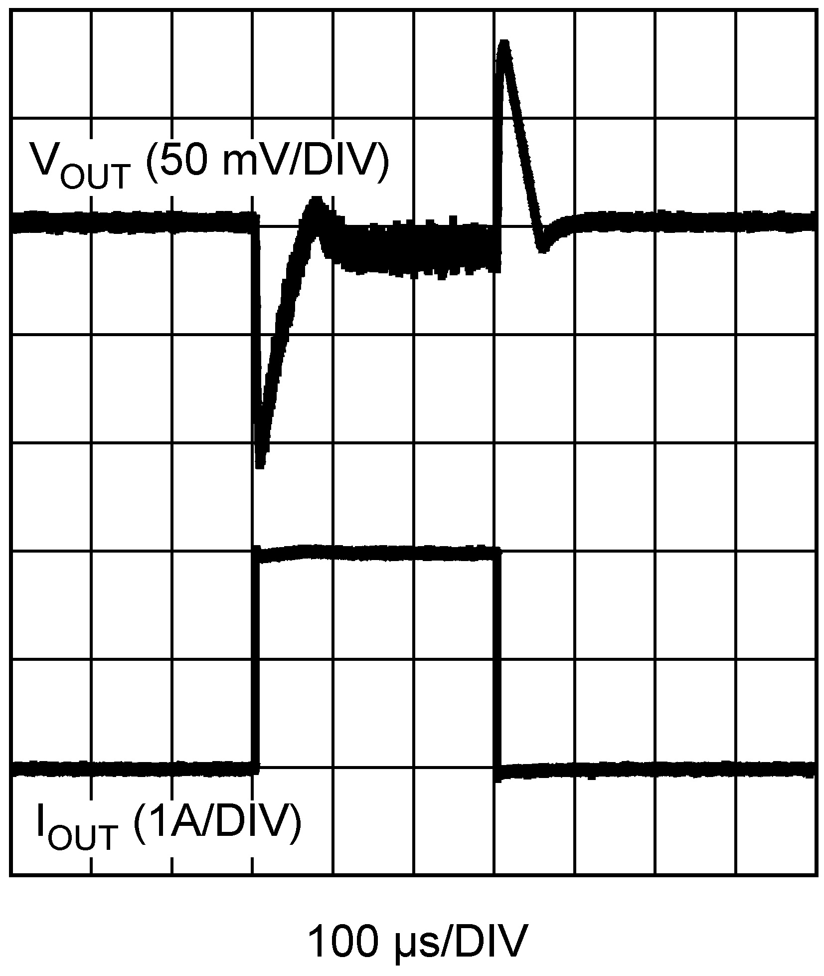
8.2.5 LM2734x Configuration From VIN = 5 V to 16 V, VOUT = 3.3 V For Full Load at 2 MHz
With SYNC = 1 MHz

| VIN = 5 V to 16 V, VOUT = 3.3 V | fSW = 1 MHz | IOUT = Full load |
For Full Load at 2 MHz With SYNC = 1-MHz Schematic
8.2.5.1 Design Requirements
Create 1.8-V output at full-rated load for VIN range of 5 V to 16 V with switching frequency FSW = 1 MHz using external synchronization.
8.2.5.2 Detailed Design Procedure
The device must be able to operate at any voltage within the recommended operating range. The load current must be defined to properly size the inductor, input, and output capacitors. The inductor must be able to handle the full expected load current as well as the peak current generated during load transients and start-up. The inrush current at start-up depends on the output capacitor selection.
Table 12 lists the bill of materials for VIN = 5 V to 16 V, VOUT = 3.3 V for full load at 2 MHz with SYNC = 1 MHz. See Figure 46.
Table 12. Bill of Materials
| PART NAME | PART ID | PART VALUE | PART NUMBER | MANUFACTURER |
|---|---|---|---|---|
| Buck regulator | U1 | 1.5-A or 2-A Buck regulator | LM2734x and LM2734x-Q1 | TI |
| CPVIN | C1 | 10 µF | GRM32DR71E106KA12L | Murata |
| CBOOST | C2 | 0.1 µF | GRM188R71C104KA01D | Murata |
| COUT | C3 | 47 µF | GRM32ER61A476KE20L | Murata |
| COUT | C4 | 22 µF | C3225X7R1C226K | TDK |
| CFF | C5 | 0.27 µF | C0603C274K4RACTU | Kemet |
| Catch diode | D1 | Schottky diode, Vf = 0.32 V | CMS06 | Toshiba |
| Inductor | L1 | 2.7 µH | CDRH5D18BHPNP | Sumida |
| Feedback resistor | R1 | 430 Ω | CRCW0603430RFKEA | Vishay |
| Feedback resistor | R2 | 187 Ω | CRCW0603187RFKEA | Vishay |
8.2.5.3 Application Curves
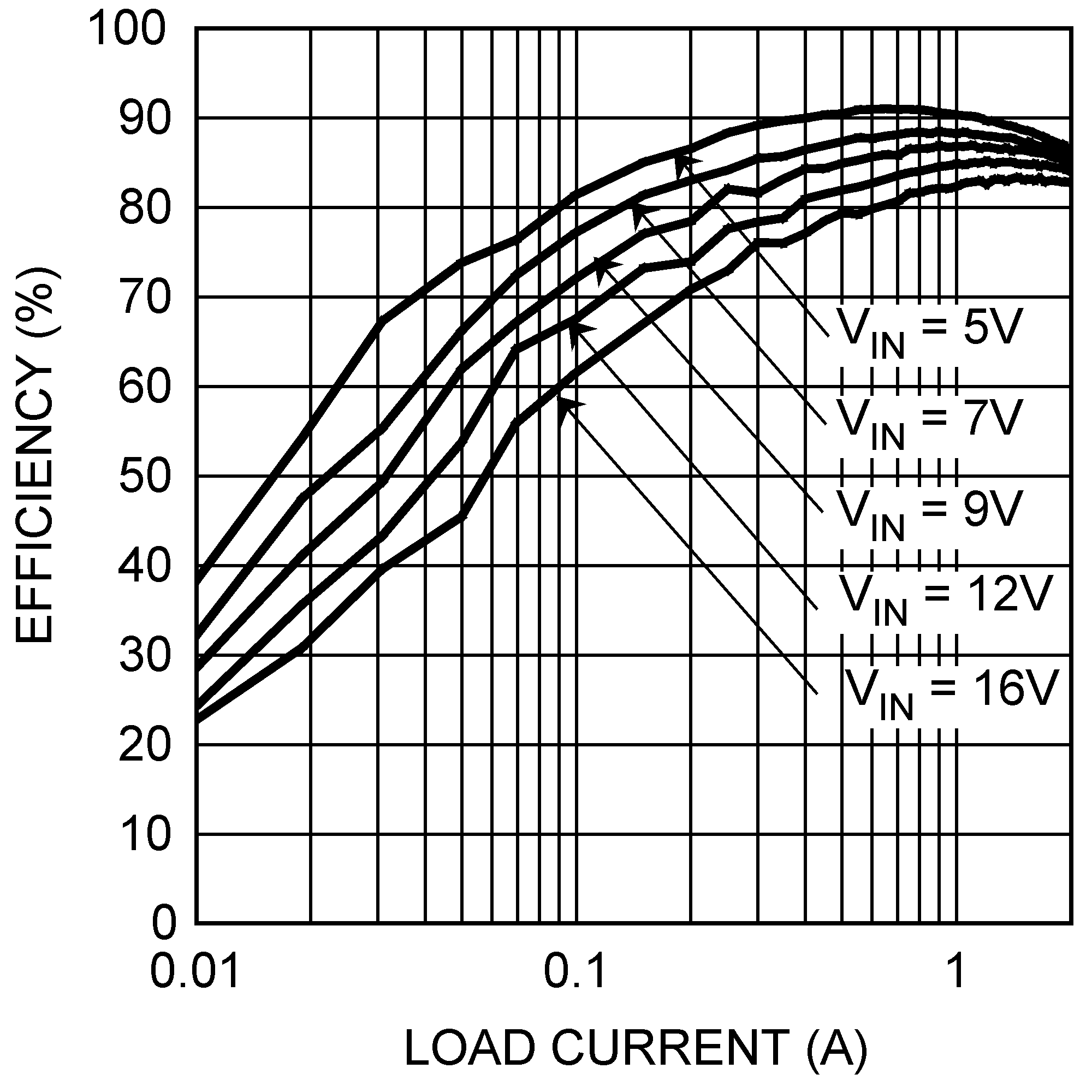 Figure 47. LM27342 Efficiency vs Load Current
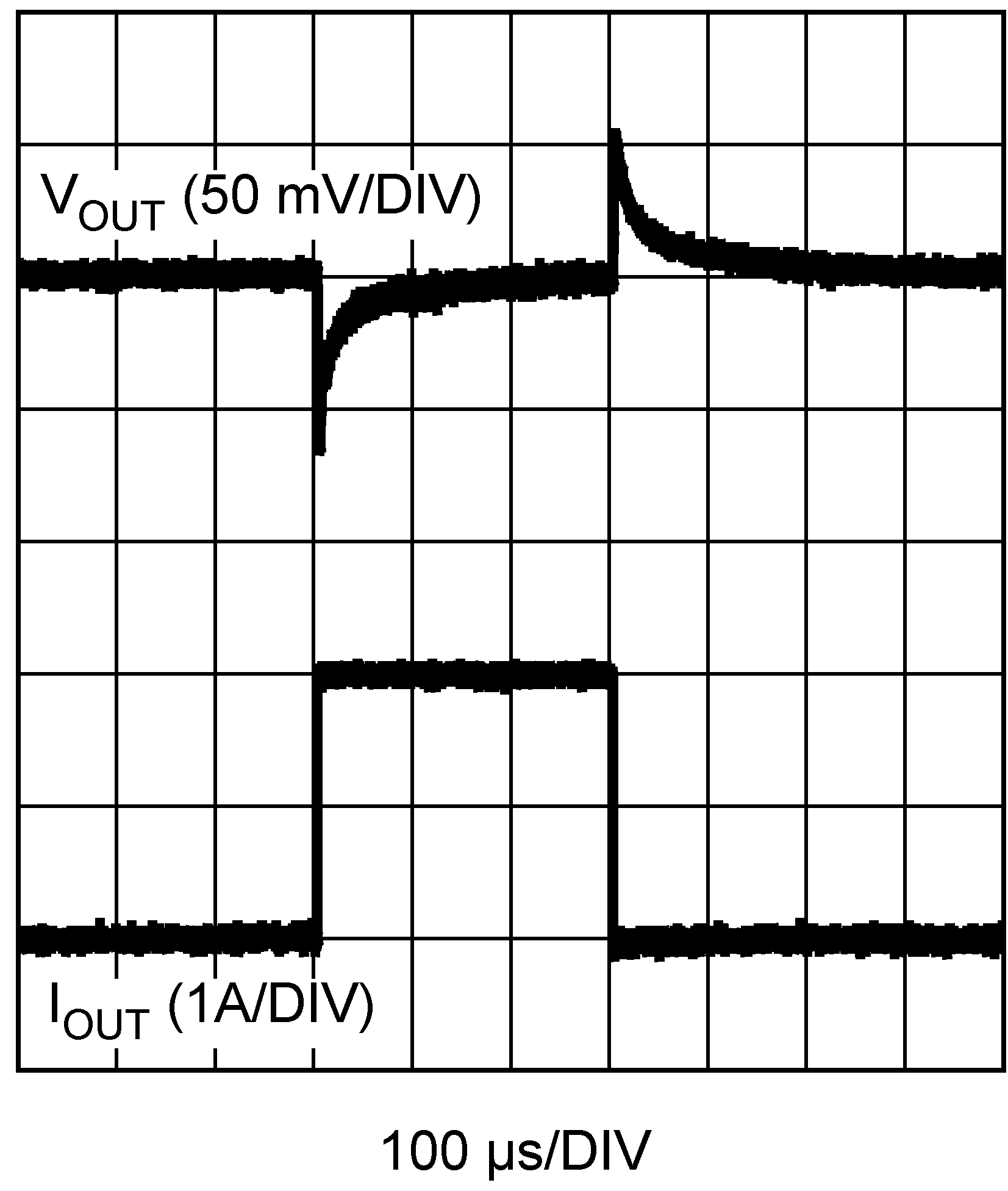
8.2.6 LM2734x Configuration From VIN = 3.3 V to 16 V, VOUT = 1.8 V For Full Load at 2 MHz
With SYNC = 1 GND

| VIN = 3.3 V to 16 V, VOUT = 1.8 V | fSW = 2 MHz | IOUT = Full load |
For Full Load at 2 MHz With SYNC = GND Schematic
8.2.6.1 Design Requirements
Create 1.8-V output at full-rated load for VIN range of 3.3 V to 16 V with switching frequency FSW = 2 MHz using internal oscillator.
8.2.6.2 Detailed Design Procedure
The device must be able to operate at any voltage within the recommended operating range. The load current must be defined to properly size the inductor, input, and output capacitors. The inductor must be able to handle the full expected load current as well as the peak current generated during load transients and start-up. The inrush current at start-up depends on the output capacitor selection.
Table 13 lists the bill of materials for VIN = 3.3 V to 16 V, VOUT = 1.8 V for full load at 2 MHz with SYNC = GND. See Figure 49.
Table 13. Bill of Materials
| PART NAME | PART ID | PART VALUE | PART NUMBER | MANUFACTURER |
|---|---|---|---|---|
| Buck regulator | U1 | 1.5-A or 2-A Buck regulator | LM2734x and LM2734x-Q1 | TI |
| CPVIN | C1 | 10 µF | GRM32DR71E106KA12L | Murata |
| CBOOST | C2 | 0.1 µF | GRM188R71C104KA01D | Murata |
| COUT | C3 | 22 µF | C3225X7R1C226K | TDK |
| COUT | C4 | 22 µF | C3225X7R1C226K | TDK |
| Catch diode | D1 | Schottky diode, Vf = 0.32 V | CMS06 | Toshiba |
| Inductor | L1 | 1 µH | CDRH5D18BHPNP | Sumida |
| Feedback resistor | R1 | 12 kΩ | CRCW060312K0FKEA | Vishay |
| Feedback resistor | R2 | 15 kΩ | CRCW060315K0FKEA | Vishay |
8.2.6.3 Application Curves
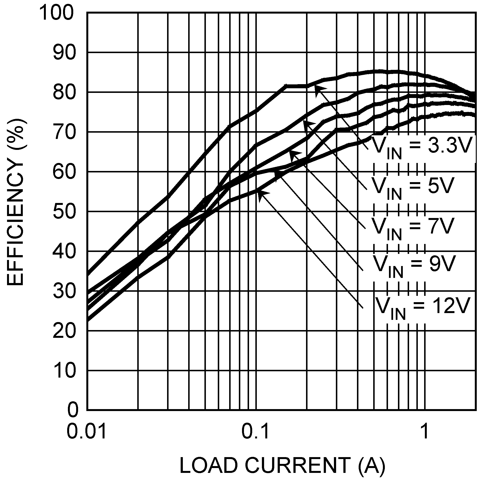 Figure 50. LM27342 Efficiency vs Load Current
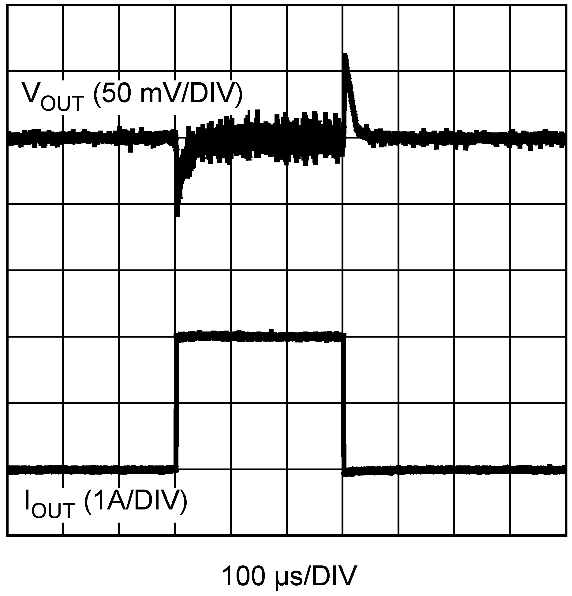
8.2.7 LM2734x Configuration From VIN = 3.3 V to 16 V, VOUT = 1.8 V For Full Load at 2 MHz
With SYNC = 1 MHz

| VIN = 3.3 V to 16 V, VOUT = 1.8 V | fSW = 1 MHz | IOUT = Full load |
For Full Load at 2 MHz With SYNC = 1-MHz Schematic
8.2.7.1 Design Requirements
Create 1.8-V output at full-rated load for VIN range of 3.3 V to 16 V with switching frequency FSW = 1 MHz using external synchronization.
8.2.7.2 Detailed Design Procedure
The device must be able to operate at any voltage within the recommended operating range. The load current must be defined to properly size the inductor, input, and output capacitors. The inductor must be able to handle the full expected load current as well as the peak current generated during load transients and start-up. The inrush current at start-up depends on the output capacitor selection.
Table 14 lists the bill of materials for VIN = 3.3 V to 16 V, VOUT = 1.8 V for full load at 2 MHz with SYNC = 1 MHz. See Figure 52.
Table 14. Bill of Materials
| PART NAME | PART ID | PART VALUE | PART NUMBER | MANUFACTURER |
|---|---|---|---|---|
| Buck regulator | U1 | 1.5-A or 2-A Buck regulator | LM2734x and LM2734x-Q1 | TI |
| CPVIN | C1 | 10 µF | GRM32DR71E106KA12L | Murata |
| CBOOST | C2 | 0.1 µF | GRM188R71C104KA01D | Murata |
| COUT | C3 | 22 µF | C3225X7R1C226K | TDK |
| COUT | C4 | 22 µF | C3225X7R1C226K | TDK |
| CFF | C5 | 3.9 nF | GRM188R71H392KA01D | Murata |
| Catch diode | D1 | Schottky diode, Vf = 0.32 V | CMS06 | Toshiba |
| Inductor | L1 | 1.8 µH | CDRH5D18BHPNP | Sumida |
| Feedback resistor | R1 | 12 kΩ | CRCW060312K0FKEA | Vishay |
| Feedback resistor | R2 | 15 kΩ | CRCW060315K0FKEA | Vishay |
8.2.7.3 Application Curves
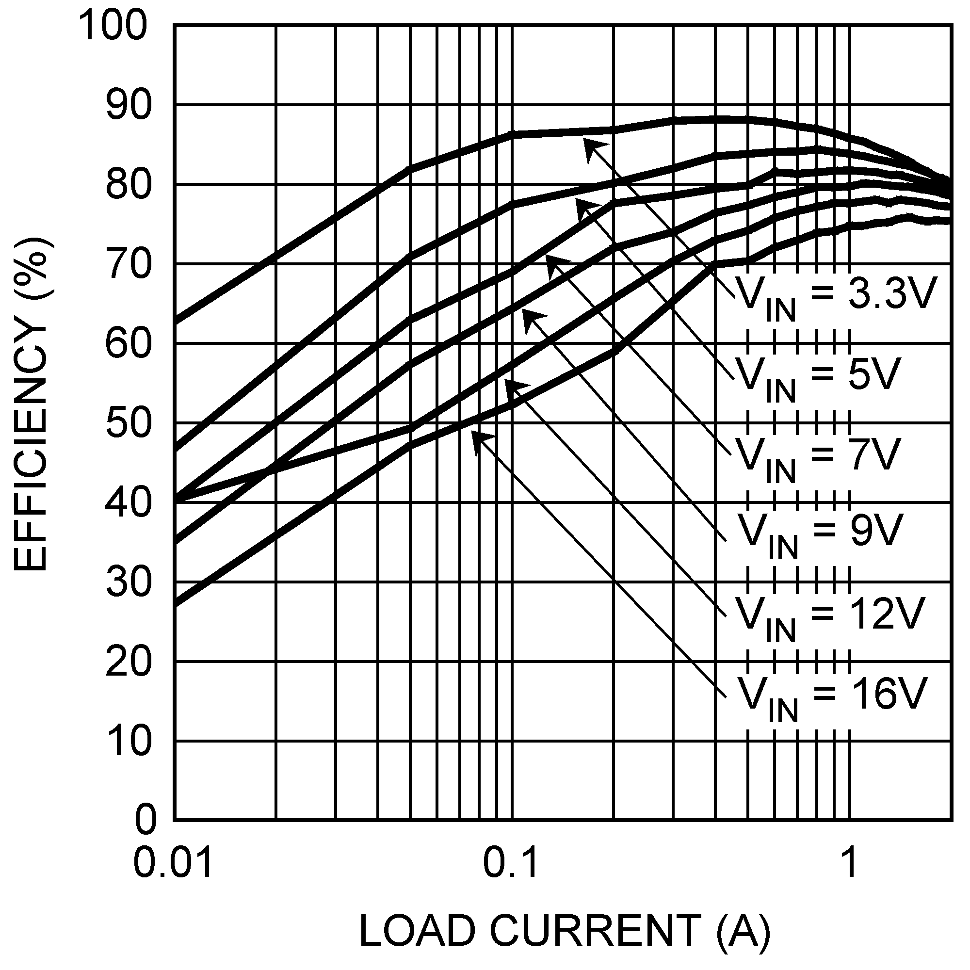 Figure 53. LM27342 Efficiency vs Load Current
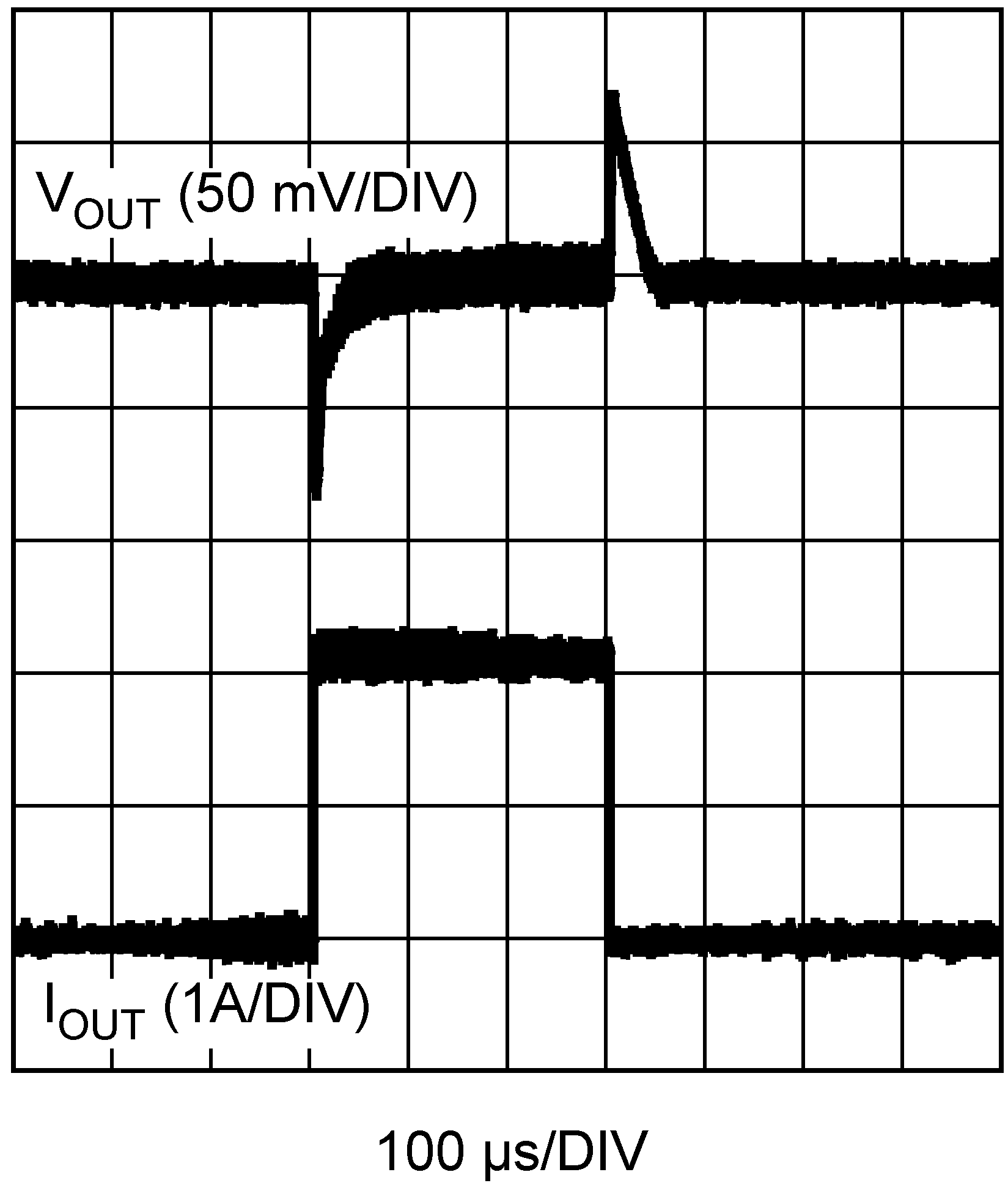
8.2.8 LM2734x Configuration From VIN = 3.3 V to 9 V, VOUT = 1.2 V For Full Load at 2 MHz
With SYNC = 2 MHz

| VIN = 3.3 V to 9 V, VOUT = 1.2 V | fSW = 2 MHz | IOUT = Full load |
For Full Load at 2 MHz With SYNC = 2-MHz Schematic
8.2.8.1 Design Requirements
Create 1.2-V output at full-rated load for VIN range of 3.3 V to 9 V with switching frequency FSW = 2 MHz using external synchronization.
8.2.8.2 Detailed Design Procedure
The device must be able to operate at any voltage within the recommended operating range. The load current must be defined to properly size the inductor, input, and output capacitors. The inductor must be able to handle the full expected load current as well as the peak current generated during load transients and start-up. The inrush current at start-up depends on the output capacitor selection.
Table 15 lists the bill of materials for VIN = 3.3 V to 9 V, VOUT = 1.2 V for full load at 2 MHz with SYNC = 2 MHz. See Figure 55.
Table 15. Bill of Materials
| PART NAME | PART ID | PART VALUE | PART NUMBER | MANUFACTURER |
|---|---|---|---|---|
| Buck regulator | U1 | 1.5-A or 2-A Buck regulator | LM2734x and LM2734x-Q1 | TI |
| CPVIN | C1 | 10 µF | GRM32DR71E106KA12L | Murata |
| CBOOST | C2 | 0.1 µF | GRM188R71C104KA01D | Murata |
| COUT | C3 | 47 µF | GRM32ER61A476KE20L | Murata |
| COUT | C4 | 22 µF | C3225X7R1C226K | TDK |
| CFF | C5 | Not mounted | ||
| Catch diode | D1 | Schottky diode, Vf = 0.32 V | CMS06 | Toshiba |
| Inductor | L1 | 0.56 µH | CDRH2D18/HPNP | Sumida |
| Feedback resistor | R1 | 1.02 kΩ | CRCW06031K02FKEA | Vishay |
| Feedback resistor | R2 | 5.1 kΩ | CRCW06035K10FKEA | Vishay |
8.2.8.3 Application Curves
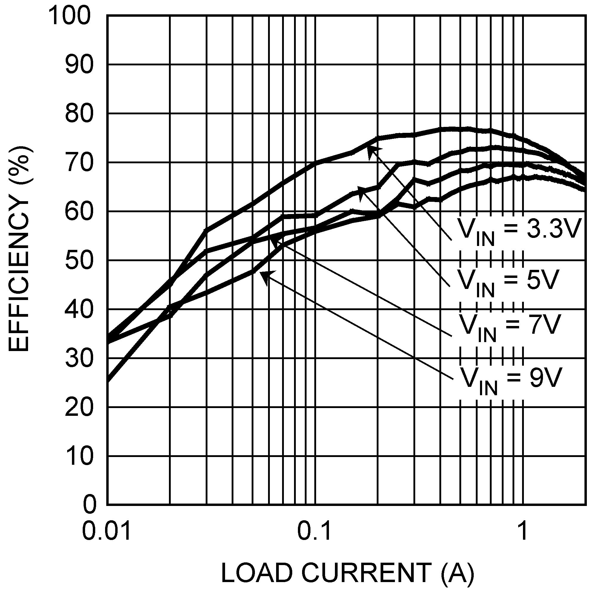 Figure 56. LM27342 Efficiency vs Load Current
