SNVS497F November 2008 – September 2016 LM27341 , LM27341-Q1 , LM27342 , LM27342-Q1
PRODUCTION DATA.
- 1 Features
- 2 Applications
- 3 Description
- 4 Revision History
- 5 Pin Configuration and Functions
- 6 Specifications
- 7 Detailed Description
-
8 Application and Implementation
- 8.1
Application Information
- 8.1.1 Inductor Selection
- 8.1.2 Inductor Material Selection
- 8.1.3 Input Capacitor
- 8.1.4 Output Capacitor
- 8.1.5 Catch Diode
- 8.1.6 Boost Diode (Optional)
- 8.1.7 Boost Capacitor
- 8.1.8 Output Voltage
- 8.1.9 Feedforward Capacitor (Optional)
- 8.1.10
Calculating Efficiency and Junction Temperature
- 8.1.10.1 Schottky Diode Conduction Losses
- 8.1.10.2 Inductor Conduction Losses
- 8.1.10.3 MOSFET Conduction Losses
- 8.1.10.4 MOSFET Switching Losses
- 8.1.10.5 IC Quiescent Losses
- 8.1.10.6 MOSFET Driver Losses
- 8.1.10.7 Total Power Losses
- 8.1.10.8 Efficiency Calculation Example
- 8.1.10.9 Calculating Junction Temperature
- 8.2
Typical Applications
- 8.2.1 LM2734x Configuration From VIN = 7 V to 16 V, VOUT = 5 V For Full Load at 2 MHz
- 8.2.2 LM2734x Configuration From VIN = 7 V to 16 V, VOUT = 5 V For Full Load at 1 MHz
- 8.2.3 LM2734x Configuration From VIN = 5 V to 16 V, VOUT = 3.3 V For Full Load at 2 MHz
- 8.2.4 LM2734x Configuration From VIN = 5 V to 16 V, VOUT = 3.3 V For Full Load at 2 MHz With SYNC = GND
- 8.2.5 LM2734x Configuration From VIN = 5 V to 16 V, VOUT = 3.3 V For Full Load at 2 MHz With SYNC = 1 MHz
- 8.2.6 LM2734x Configuration From VIN = 3.3 V to 16 V, VOUT = 1.8 V For Full Load at 2 MHz With SYNC = 1 GND
- 8.2.7 LM2734x Configuration From VIN = 3.3 V to 16 V, VOUT = 1.8 V For Full Load at 2 MHz With SYNC = 1 MHz
- 8.2.8 LM2734x Configuration From VIN = 3.3 V to 9 V, VOUT = 1.2 V For Full Load at 2 MHz With SYNC = 2 MHz
- 8.1
Application Information
- 9 Power Supply Recommendations
- 10Layout
- 11Device and Documentation Support
- 12Mechanical, Packaging, and Orderable Information
10 Layout
10.1 Layout Guidelines
10.1.1 Compact Layout
The performance of any switching converter depends as much upon the layout of the PCB as the component selection. The following guidelines help the user design a circuit with maximum rejection of outside EMI and minimum generation of unwanted EMI.
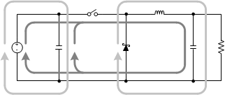
Parasitic inductance can be reduced by keeping the power path components close together and keeping the area of the loops small, on which high currents travel. Short, thick traces or copper pours (shapes) are best. In particular, the switch node (where L1, D1, and the SW pin connect) must be just large enough to connect all three components without excessive heating from the current it carries. The LM2734x and LM2734x-Q1 operate in two distinct cycles (see Figure 27) whose high current paths are shown in Figure 58.
 Figure 58. Buck Converter Current Loops
The dark grey, inner loop represents the high current path during the MOSFET on-time. The light grey, outer loop represents the high current path during the off-time.
10.1.2 Ground Plane and Shape Routing
The diagram of Figure 58 is also useful for analyzing the flow of continuous current versus the flow of pulsating currents. The circuit paths with current flow during both the on-time and off-time are considered to be continuous current, while those that carry current during the on-time or off-time only are pulsating currents. Preference in routing must be given to the pulsating current paths, as these are the portions of the circuit most likely to emit EMI. The ground plane of a PCB is a conductor and return path, and it is susceptible to noise injection just like any other circuit path. The path between the input source and the input capacitor and the path between the catch diode and the load are examples of continuous current paths. In contrast, the path between the catch diode and the input capacitor carries a large pulsating current. This path must be routed with a short, thick shape, preferably on the component side of the PCB. Multiple vias in parallel must be used right at the pad of the input capacitor to connect the component side shapes to the ground plane. A second pulsating current loop that is often ignored is the gate drive loop formed by the SW and BOOST pins and boost capacitor CBOOST. To minimize this loop and the EMI it generates, keep CBOOST close to the SW and BOOST pins.
10.1.3 FB Loop
The FB pin is a high-impedance input, and the loop created by R2, the FB pin and ground must be made as small as possible to maximize noise rejection. R2 must therefore be placed as close as possible to the FB and GND pins of the IC.
10.1.4 PCB Summary
- Minimize the parasitic inductance by keeping the power path components close together and keeping the area of the high-current loops small.
- The most important consideration when completing the layout is the close coupling of the GND connections of the CIN capacitor and the catch diode D1. These ground connections must be immediately adjacent, with multiple vias in parallel at the pad of the input capacitor connected to GND. Place CIN and D1 as close to the IC as possible.
- Next in importance is the location of the GND connection of the COUT capacitor, which must be near the GND connections of CIN and D1.
- There must be a continuous ground plane on the copper layer directly beneath the converter. This reduces parasitic inductance and EMI.
- The FB pin is a high impedance node and care must be taken to make the FB trace short to avoid noise pickup and inaccurate regulation. The feedback resistors must be placed as close as possible to the IC, with the GND of R2 placed as close as possible to the GND of the IC. The VOUT trace to R1 must be routed away from the inductor and any other traces that are switching.
- High AC currents flow through the VIN, SW and VOUT traces, so they must be as short and wide as possible. However, making the traces wide increases radiated noise, so the layout designer must make this trade-off. Radiated noise can be decreased by choosing a shielded inductor.
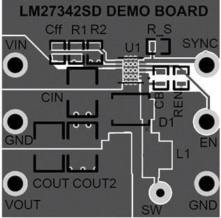
The remaining components must also be placed as close as possible to the IC. See AN-1229 SIMPLE SWITCHER® PCB Layout Guidelines (SNVA054) for further considerations and the LM27342 demo board as an example of a four-layer layout.
10.2 Layout Example
 Figure 59. Top Layer and Overlay