SNVS334F January 2005 – January 2016 LM2734Z , LM2734Z-Q1
PRODUCTION DATA.
- 1 Features
- 2 Applications
- 3 Description
- 4 Revision History
- 5 Pin Configuration and Functions
- 6 Specifications
- 7 Detailed Description
-
8 Application and Implementation
- 8.1 Application Information
- 8.2
Typical Applications
- 8.2.1
LM2734Z Design Example 1
- 8.2.1.1 Design Requirements
- 8.2.1.2
Detailed Design Procedure
- 8.2.1.2.1 Inductor Selection
- 8.2.1.2.2 Input Capacitor
- 8.2.1.2.3 Output Capacitor
- 8.2.1.2.4 Catch Diode
- 8.2.1.2.5 Boost Diode
- 8.2.1.2.6 Boost Capacitor
- 8.2.1.2.7 Output Voltage
- 8.2.1.2.8 Calculating Efficiency, and Junction Temperature
- 8.2.1.2.9 Calculating the LM2734Z Junction Temperature
- 8.2.1.2.10 WSON Package
- 8.2.1.2.11 Package Selection
- 8.2.1.3 Application Curve
- 8.2.2 LM2734Z Design Example 2
- 8.2.3 LM2734Z Design Example 3
- 8.2.4 LM2734Z Design Example 4
- 8.2.5 LM2734Z Design Example 5
- 8.2.1
LM2734Z Design Example 1
- 9 Power Supply Recommendations
- 10Layout
- 11Device and Documentation Support
- 12Mechanical, Packaging, and Orderable Information
6 Specifications
6.1 Absolute Maximum Ratings
See (1)(2)(1) Stresses beyond those listed under Absolute Maximum Ratings may cause permanent damage to the device. These are stress ratings only, which do not imply functional operation of the device at these or any other conditions beyond those indicated under Recommended Operating Conditions. Exposure to absolute-maximum-rated conditions for extended periods may affect device reliability.
(2) If Military/Aerospace specified devices are required, please contact the Texas Instruments Sales Office/ Distributors for availability and specifications.
6.2 ESD Ratings
| VALUE | UNIT | ||||
|---|---|---|---|---|---|
| V(ESD) | Electrostatic discharge | Human-body model (HBM), per AEC Q100-002(1)(2) | ±2000 | V | |
| Charged-device model (CDM), per AEC Q100-002 | ±1000 | ||||
(1) AEC Q100-002 indicates that HBM stressing shall be in accordance with the ANSI/ESDA/JEDEC JS-001 specification.
(2) Human-body model, 1.5 kΩ in series with 100 pF.
6.3 Recommended Operating Conditions
| MIN | MAX | UNIT | |||
|---|---|---|---|---|---|
| VIN | Input voltage | 3 | 20 | V | |
| SW voltage | –0.5 | 20 | V | ||
| Boost voltage | –0.5 | 25 | V | ||
| Boost to SW voltage | 1.6 | 5.5 | V | ||
| TJ | Junction temperature | –40 | 125 | °C | |
6.4 Thermal Information
| THERMAL METRIC(1) | LM2734Z | UNIT | ||
|---|---|---|---|---|
| DDC (SOT) | NGG (WSON) | |||
| 6 PINS | 6 PINS | |||
| RθJA | Junction-to-ambient thermal resistance(2) | 180.3 | 56.2 | °C/W |
| RθJC(top) | Junction-to-case (top) thermal resistance | 51.6 | 52.6 | °C/W |
| RθJB | Junction-to-board thermal resistance | 27.7 | 30.7 | °C/W |
| ψJT | Junction-to-top characterization parameter | 1.2 | 0.9 | °C/W |
| ψJB | Junction-to-board characterization parameter | 27.3 | 30.8 | °C/W |
| RθJC(bot) | Junction-to-case (bottom) thermal resistance | — | 10.7 | °C/W |
(1) For more information about traditional and new thermal metrics, see the Semiconductor and IC Package Thermal Metrics application report (SPRA953).
(2) Thermal shutdown occurs if the junction temperature exceeds 165°C. The maximum power dissipation is a function of TJ(MAX), RθJA and TA . The maximum allowable power dissipation at any ambient temperature is PD = (TJ(MAX) – TA)/RθJA . All numbers apply for packages soldered directly onto a 3-in × 3-in printed-circuit-board with 2-oz. copper on 4 layers in still air. For a 2-layer board using 1-oz. copper in still air, RθJA = 204°C/W.
6.5 Electrical Characteristics
All typical specifications are for TJ = 25°C, and all maximum and minimum limits apply over the full operating temperature range (TJ = –40°C to 125°C). VIN = 5 V, VBOOST – VSW = 5 V (unless otherwise noted). Data sheet minimum and maximum specification limits are specified by design, test, or statistical analysis.| PARAMETER | TEST CONDITIONS | MIN(1) | TYP(2) | MAX(1) | UNIT | ||
|---|---|---|---|---|---|---|---|
| VFB | Feedback voltage | 0.784 | 0.8 | 0.816 | V | ||
| ΔVFB/ΔVIN | Feedback voltage line regulation | VIN = 3 V to 20 V | 0.01 | % / V | |||
| IFB | Feedback input bias current | Sink and source | 10 | 250 | nA | ||
| UVLO | Undervoltage lockout | VIN Rising | 2.74 | 2.90 | V | ||
| Undervoltage lockout | VIN Falling | 2 | 2.3 | ||||
| UVLO hysteresis | 0.30 | 0.44 | 0.62 | ||||
| FSW | Switching frequency | 2.2 | 3.0 | 3.6 | MHz | ||
| DMAX | Maximum duty cycle | 78% | 85% | ||||
| DMIN | Minimum duty Cycle | 8% | |||||
| RDS(ON) | Switch ON resistance | VBOOST - VSW = 3 V (SOT Package) |
300 | 600 | mΩ | ||
| VBOOST - VSW = 3 V (WSON Package) |
340 | 650 | mΩ | ||||
| ICL | Switch current limit | VBOOST - VSW = 3 V | 1.2 | 1.7 | 2.5 | A | |
| IQ | Quiescent current | Switching | 1.5 | 2.5 | mA | ||
| Quiescent current (shutdown) | VEN = 0 V | 30 | nA | ||||
| IBOOST | Boost pin current | (Switching) | 4.25 | 6 | mA | ||
| VEN_TH | Shutdown threshold voltage | VEN Falling | 0.4 | V | |||
| Enable threshold voltage | VEN Rising | 1.8 | |||||
| IEN | Enable pin current | Sink/source | 10 | nA | |||
| ISW | Switch leakage | 40 | nA | ||||
(1) Specified to Texas Instruments' Average Outgoing Quality Level (AOQL).
(2) Typicals represent the most likely parametric norm.
6.6 Typical Characteristics
at VIN = 5 V, VBOOST - VSW = 5 V, L1 = 2.2 µH and TA = 25°C (unless otherwise noted)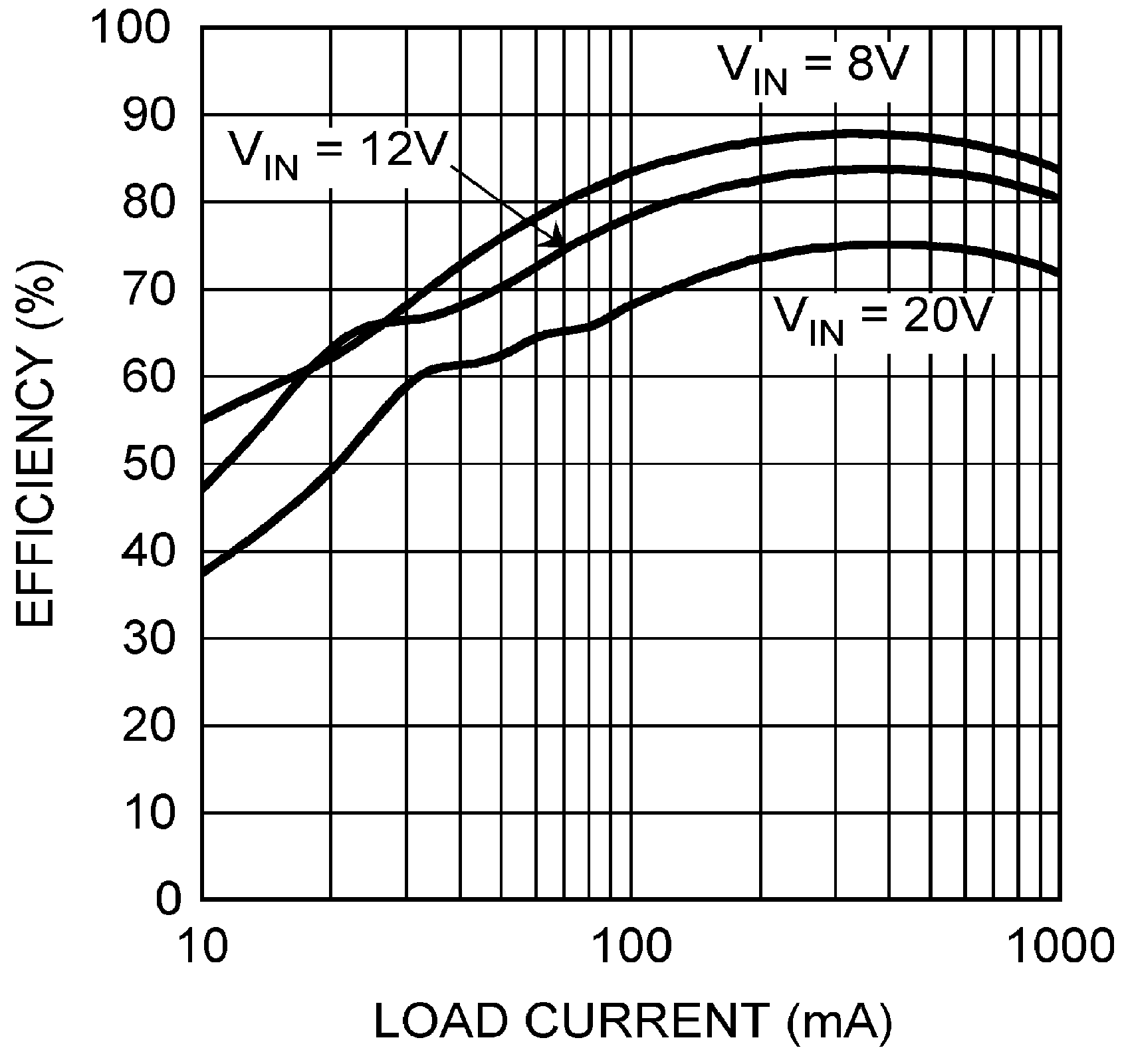
| VOUT = 5 V |
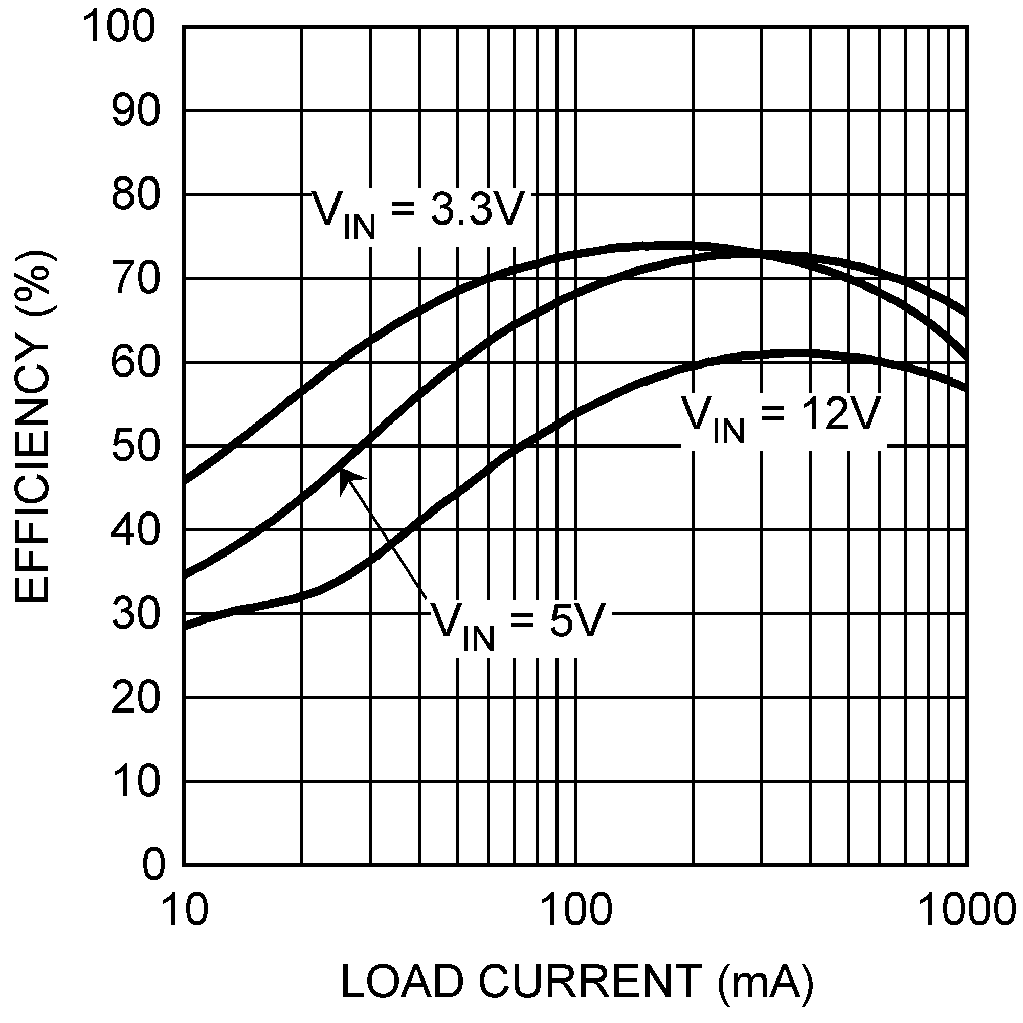
| VOUT = 1.5 V |
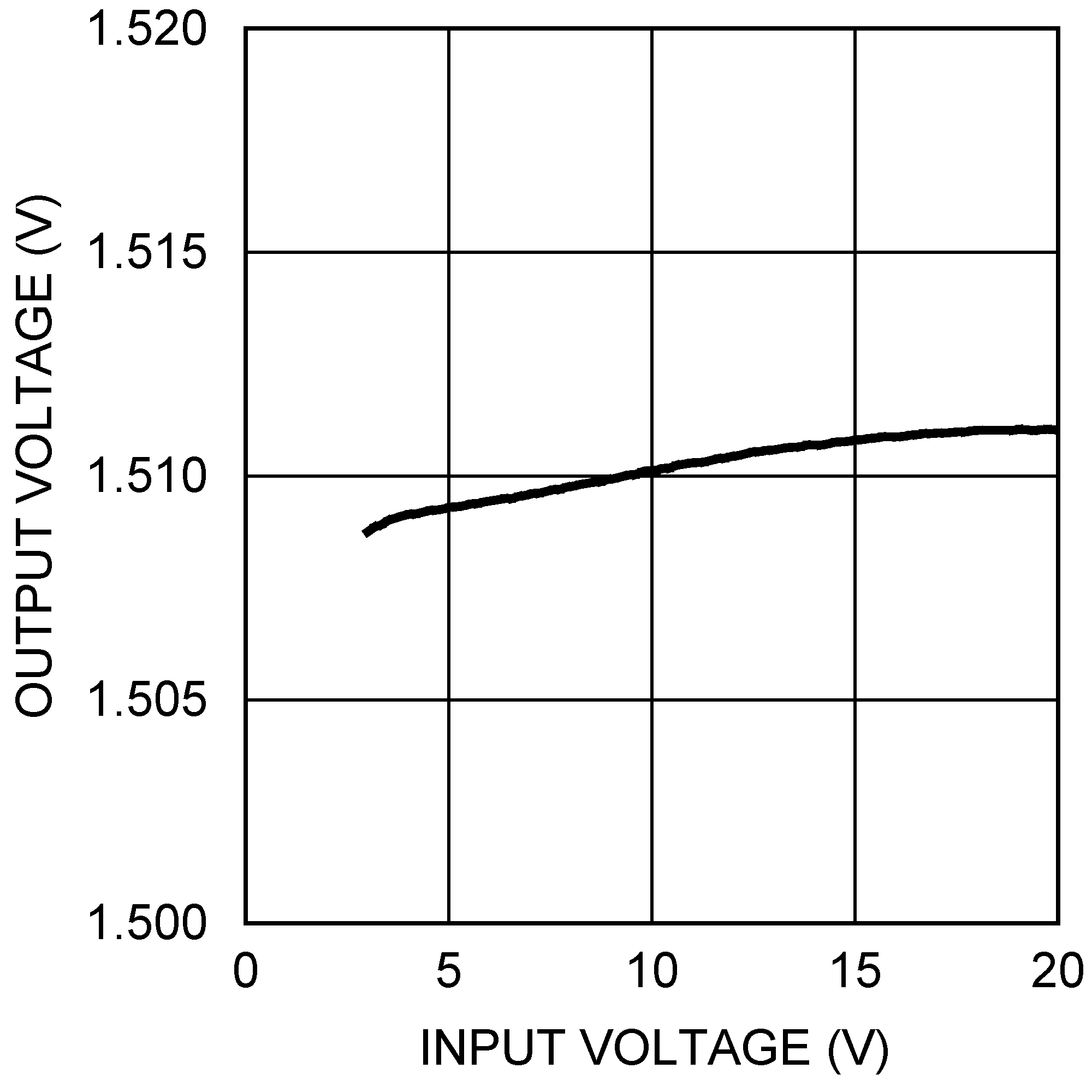
| VOUT = 1.5 V | IOUT = 500 mA |
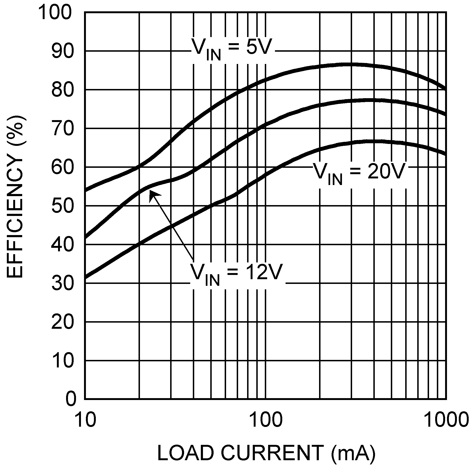
| VOUT = 3.3 V |
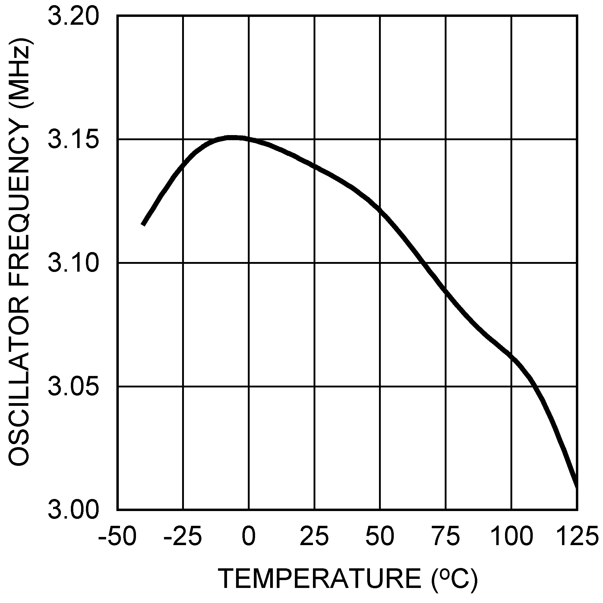
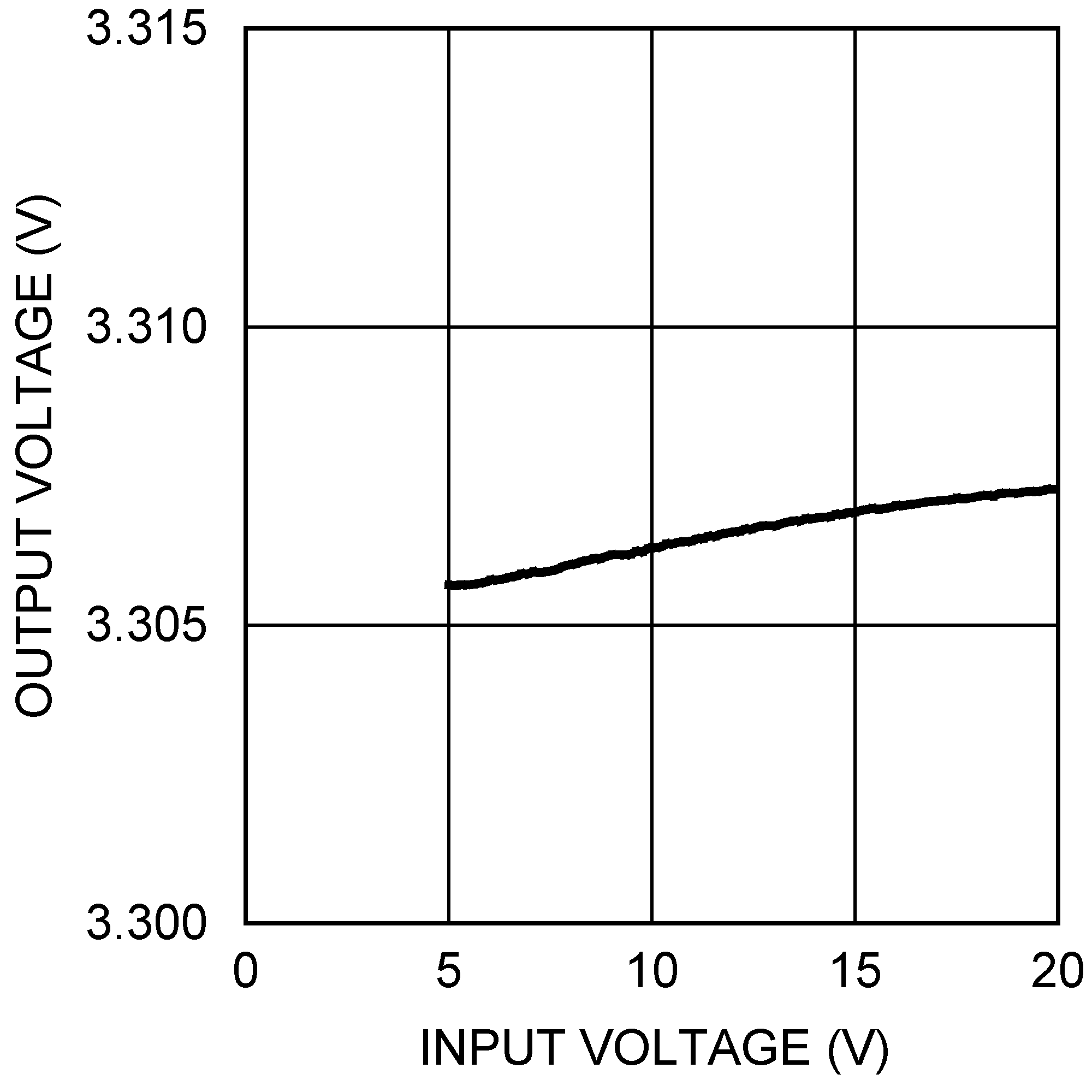
| VOUT = 3.3 V | IOUT = 500 mA |