ZHCSIR2 September 2018 LM2735-Q1
PRODUCTION DATA.
- 1 特性
- 2 应用
- 3 说明
- 4 修订历史记录
- 5 Pin Configuration and Functions
- 6 Specifications
- 7 Detailed Description
-
8 Application and Implementation
- 8.1 Application Information
- 8.2
Typical Applications
- 8.2.1 LM2735X-Q1 SOT-23 Design Example 1
- 8.2.2 LM2735Y-Q1 SOT-23 Design Example 2
- 8.2.3 LM2735X-Q1 WSON Design Example 3
- 8.2.4 LM2735Y-Q1 WSON Design Example 4
- 8.2.5 LM2735X-Q1 SOT-23 Design Example 6
- 8.2.6 LM2735Y-Q1 SOT-23 Design Example 7
- 8.2.7 LM2735X-Q1 SOT-23 Design Example 8
- 8.2.8 LM2735Y-Q1 SOT-23 Design Example 9
- 8.2.9 LM2735X-Q1 WSON Design Example 10
- 8.2.10 LM2735Y-Q1 WSON Design Example 11
- 8.2.11 LM2735X-Q1 WSON SEPIC Design Example 12
- 8.2.12 LM2735X-Q1 SOT-23 LED Design Example 14
- 8.2.13 LM2735Y-Q1 WSON FlyBack Design Example 15
- 8.2.14 LM2735X-Q1 SOT-23 LED Design Example 16 VRAIL > 5.5 V Application
- 8.2.15 LM2735X-Q1 SOT-23 LED Design Example 17 Two-Input Voltage Rail Application
- 8.2.16 SEPIC Converter
- 9 Power Supply Recommendations
- 10Layout
- 11器件和文档支持
- 12机械、封装和可订购信息
7.1.1 Theory of Operation
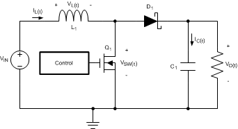
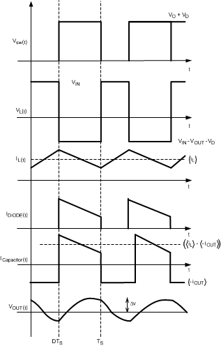
The LM2735-Q1 is a constant-frequency PWM boost regulator IC that delivers a minimum of 2.1 A peak switch current. The regulator has a preset switching frequency of either 520 kHz or 1.6 MHz. This high frequency allows the device to operate with small surface mount capacitors and inductors, resulting in a DC/DC converter that requires a minimum amount of board space. The LM2735-Q1 is internally compensated, so it is simple to use, and requires few external components. The device uses current-mode control to regulate the output voltage. The following operating description of the LM2735-Q1 refers to the simplified internal block diagram (Functional Block Diagram), the simplified schematic (Figure 13), and its associated waveforms (Figure 14). The LM2735-Q1 supplies a regulated output voltage by switching the internal NMOS control switch at constant frequency and variable duty cycle. A switching cycle begins at the falling edge of the reset pulse generated by the internal oscillator. When this pulse goes low, the output control logic turns on the internal NMOS control switch. During this on-time, the SW pin voltage (VSW) decreases to approximately GND, and the inductor current (IL) increases with a linear slope. IL is measured by the current sense amplifier, which generates an output proportional to the switch current. The sensed signal is summed with the corrective ramp of the regulator and compared to the error amplifier’s output, which is proportional to the difference between the feedback voltage and VREF. When the PWM comparator output goes high, the output switch turns off until the next switching cycle begins. During the switch off-time, inductor current discharges through diode D1, which forces the SW pin to swing to the output voltage plus the forward voltage (VD) of the diode. The regulator loop adjusts the duty cycle (D) to maintain a constant output voltage .
 Figure 13. Simplified Schematic
  Figure 14. Typical Waveforms