ZHCSIR2 September 2018 LM2735-Q1
PRODUCTION DATA.
- 1 特性
- 2 应用
- 3 说明
- 4 修订历史记录
- 5 Pin Configuration and Functions
- 6 Specifications
- 7 Detailed Description
-
8 Application and Implementation
- 8.1 Application Information
- 8.2
Typical Applications
- 8.2.1 LM2735X-Q1 SOT-23 Design Example 1
- 8.2.2 LM2735Y-Q1 SOT-23 Design Example 2
- 8.2.3 LM2735X-Q1 WSON Design Example 3
- 8.2.4 LM2735Y-Q1 WSON Design Example 4
- 8.2.5 LM2735X-Q1 SOT-23 Design Example 6
- 8.2.6 LM2735Y-Q1 SOT-23 Design Example 7
- 8.2.7 LM2735X-Q1 SOT-23 Design Example 8
- 8.2.8 LM2735Y-Q1 SOT-23 Design Example 9
- 8.2.9 LM2735X-Q1 WSON Design Example 10
- 8.2.10 LM2735Y-Q1 WSON Design Example 11
- 8.2.11 LM2735X-Q1 WSON SEPIC Design Example 12
- 8.2.12 LM2735X-Q1 SOT-23 LED Design Example 14
- 8.2.13 LM2735Y-Q1 WSON FlyBack Design Example 15
- 8.2.14 LM2735X-Q1 SOT-23 LED Design Example 16 VRAIL > 5.5 V Application
- 8.2.15 LM2735X-Q1 SOT-23 LED Design Example 17 Two-Input Voltage Rail Application
- 8.2.16 SEPIC Converter
- 9 Power Supply Recommendations
- 10Layout
- 11器件和文档支持
- 12机械、封装和可订购信息
10.3.1 Definitions
Heat energy is transferred from regions of high temperature to regions of low temperature through three basic mechanisms: radiation, conduction and convection.
- RadiationElectromagnetic transfer of heat between masses at different temperatures.
- ConductionTransfer of heat through a solid medium.
- ConvectionTransfer of heat through the medium of a fluid; typically air.
Conduction & Convection will be the dominant heat transfer mechanism in most applications.
- RθJCThermal impedance from silicon junction to device case temperature.
- RθJAThermal impedance from silicon junction to ambient air temperature.
- CθJCThermal Delay from silicon junction to device case temperature.
- CθCAThermal Delay from device case to ambient air temperature.
- RθJA & RθJCThese two symbols represent thermal impedances, and most data sheets contain associated values for these two symbols. The units of measurement are °C/Watt.
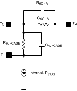
RθJAis the sum of smaller thermal impedances (see Figure 44). The capacitors represent delays that are present from the time that power and its associated heat is increased or decreased from steady state in one medium until the time that the heat increase or decrease reaches steady state on the another medium.
 Figure 44. Simplified Thermal Impedance Model
 The datasheet values for these symbols are given so that one might compare the thermal performance of one package against another. In order to achieve a comparison between packages, all other variables must be held constant in the comparison (PCB size, copper weight, thermal vias, power dissipation, VIN, VOUT, Load Current, and so forth). This does shed light on the package performance, but it would be a mistake to use these values to calculate the actual junction temperature in your application.

Calculation of the variables of Equation 29 is discussed later, as well as how to eventually calculate a proper junction temperature with relative certainty. The following defines the process of calculating the junction temperature and clarify some common misconceptions.
RθJA [Variables]:
- Input voltage, output voltage, output current, RDSon.
- Ambient temperature and air flow.
- Internal and external components power dissipation.
- Package thermal limitations.
- PCB variables (copper weight, thermal vias, layers component placement).
It is incorrect to assume that the top case temperature is the proper temperature when calculating RθJC value. The RθJC value represents the thermal impedance of all six sides of a package, not just the top side. This document refers to a thermal impedance called RψJC. RψJC represents a thermal impedance associated with just the top case temperature. This allows calculation of the junction temperature with a thermal sensor connected to the top case.