ZHCS547K January 2010 – February 2018 LM27402
PRODUCTION DATA.
- 1 特性
- 2 应用
- 3 说明
- 4 修订历史记录
- 5 Pin Configuration and Functions
- 6 Specifications
-
7 Detailed Description
- 7.1 Overview
- 7.2 Functional Block Diagram
- 7.3
Feature Description
- 7.3.1 Wide Input Voltage Range
- 7.3.2 UVLO
- 7.3.3 Precision Enable
- 7.3.4 Soft-Start and Voltage Tracking
- 7.3.5 Output Voltage Setpoint and Accuracy
- 7.3.6 Voltage-Mode Control
- 7.3.7 Power Good
- 7.3.8 Inductor-DCR-Based Overcurrent Protection
- 7.3.9 Current Sensing
- 7.3.10 Power MOSFET Gate Drivers
- 7.3.11 Pre-Bias Start-up
- 7.4 Device Functional Modes
-
8 Application and Implementation
- 8.1
Application Information
- 8.1.1 Converter Design
- 8.1.2 Inductor Selection (L)
- 8.1.3 Output Capacitor Selection (COUT)
- 8.1.4 Input Capacitor Selection (CIN)
- 8.1.5 Using Precision Enable
- 8.1.6 Setting the Soft-Start Time
- 8.1.7 Tracking
- 8.1.8 Setting the Switching Frequency
- 8.1.9 Setting the Current Limit Threshold
- 8.1.10 Control Loop Compensation
- 8.1.11 MOSFET Gate Drivers
- 8.1.12 Power Loss and Efficiency Calculations
- 8.2 Typical Applications
- 8.1
Application Information
- 9 Power Supply Recommendations
- 10Layout
- 11器件和文档支持
- 12机械、封装和可订购信息
封装选项
机械数据 (封装 | 引脚)
散热焊盘机械数据 (封装 | 引脚)
订购信息
8.1.9 Setting the Current Limit Threshold
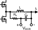
As mentioned in the Current Sensing section, the LM27402 exploits the filter inductor DCR to detect overcurrent events. If desired, the user can employ inductors with low tolerance DCR to increase the accuracy of the current limit threshold. The most common circuit arrangement for sensing the inductor DCR voltage is shown in Figure 32.
 Figure 32. Inductor DCR Current Sensing Circuit
The most accurate sensing of the differential voltage across the inductor DCR is achieved by matching the time constant of the RSCS sense filter with the inductor's L/RDCR time constant. If the time constants are matched, the voltage across the capacitor follows the voltage across the DCR. A typical range of capacitance used in the RSCS network is 100 nF to 1µF. The equation to match the time constants is:

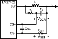
Adjust the current limit threshold to any level with a single resistor from the current limit comparator to the output voltage pin. Use the circuit in Figure 33 to set the current limit.
 Figure 33. Adjusting the Current Limit Setpoint
Because the voltage across the inductor DCR follows the current through the inductor, the device trips at the peak of the inductor current. Capacitor CSBY shown in Figure 33 filters the input to the current sense comparator. A working range for this capacitance is 47 pF to 100 pF. The equation to set the resistor value of RSET is:

ILIMIT is the desired current limit level, RDCR is the rated DC resistance of the inductor and Ics- is the 10 µA current source flowing out of the CS– pin. To aid in high frequency common-mode rejection, a series resistor, RCS, of same resistance as RSET, is optionally added to the CS+ signal path.
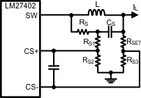
The internal current source ICS- is powered from the input voltage rail, VIN. The minimum voltage required to drive that current source is 1 V from VIN to VOUT. If a low-dropout condition occurs where VIN – VOUT< 1 V, the LM27402 may prematurely initiate hiccup mode. There are multiple options to avoid this situation. The first option is to enable the LM27402 after the input voltage has risen 1 V above the nominal output voltage as seen in Figure 28. The second option is to lower the comparator common-mode voltage shown in Figure 34 such that the ICS- current source has enough headroom voltage.
 Figure 34. Common Mode Voltage Resistor Divider Network
Refer to AN-2060 LM27402 Current Limit Application Circuits (SNVA441) for design guidelines to adjust the common-mode voltage of the current sense comparator.