ZHCS547K January 2010 – February 2018 LM27402
PRODUCTION DATA.
- 1 特性
- 2 应用
- 3 说明
- 4 修订历史记录
- 5 Pin Configuration and Functions
- 6 Specifications
-
7 Detailed Description
- 7.1 Overview
- 7.2 Functional Block Diagram
- 7.3
Feature Description
- 7.3.1 Wide Input Voltage Range
- 7.3.2 UVLO
- 7.3.3 Precision Enable
- 7.3.4 Soft-Start and Voltage Tracking
- 7.3.5 Output Voltage Setpoint and Accuracy
- 7.3.6 Voltage-Mode Control
- 7.3.7 Power Good
- 7.3.8 Inductor-DCR-Based Overcurrent Protection
- 7.3.9 Current Sensing
- 7.3.10 Power MOSFET Gate Drivers
- 7.3.11 Pre-Bias Start-up
- 7.4 Device Functional Modes
-
8 Application and Implementation
- 8.1
Application Information
- 8.1.1 Converter Design
- 8.1.2 Inductor Selection (L)
- 8.1.3 Output Capacitor Selection (COUT)
- 8.1.4 Input Capacitor Selection (CIN)
- 8.1.5 Using Precision Enable
- 8.1.6 Setting the Soft-Start Time
- 8.1.7 Tracking
- 8.1.8 Setting the Switching Frequency
- 8.1.9 Setting the Current Limit Threshold
- 8.1.10 Control Loop Compensation
- 8.1.11 MOSFET Gate Drivers
- 8.1.12 Power Loss and Efficiency Calculations
- 8.2 Typical Applications
- 8.1
Application Information
- 9 Power Supply Recommendations
- 10Layout
- 11器件和文档支持
- 12机械、封装和可订购信息
封装选项
机械数据 (封装 | 引脚)
散热焊盘机械数据 (封装 | 引脚)
订购信息
8.1.10 Control Loop Compensation
The LM27402 voltage mode control system incorporates input voltage feedforward to eliminate the input voltage dependence of the PWM modulator gain. Input voltage feedforward is essential for stability across the entire input voltage range and makes it easier for the designer to select the compensation and power train components. The following describes how to set the output voltage and obtain the open-loop transfer function.
During steady state operation, the DC output voltage is set by the feedback resistor network between VOUT, FB and GND. The FB voltage is nominally 0.6 V ±1%. The equation describing the output voltage is:

A good starting value for RFB1 is 20 kΩ. If an output voltage of 0.6 V is required, RFB2 must not be used.
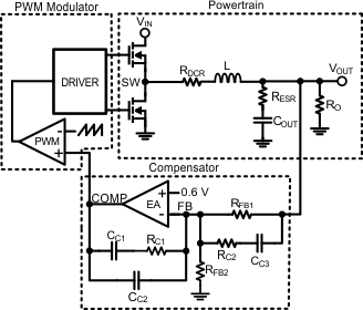
There are three main blocks of a voltage-mode buck switcher that the power supply designer needs to consider when designing the control system: power train, PWM modulator, and compensator. A diagram representing the control loop is shown in Figure 35.
 Figure 35. Control Loop Schematic Diagram
The power train consists of the filter inductor (L) with DCR (RDCR), output capacitor (COUT) with ESR (effective series resistance RESR), and effective load resistance (RO). The error amplifier (EA) regulates the feedback (FB) voltage to 0.6V. The passive compensation components around the error amplifier establish system stability. Type-III compensation is shown in Figure 35. The PWM modulator establishes the duty cycle command by comparing the error amplifier output (COMP) with an internally generated ramp set at the switching frequency.
The modulator gain, power train and compensator transfer functions must be taken into consideration when obtaining the total open-loop transfer function. The PWM modulator adds a DC gain component to the open-loop transfer function. In a basic voltage-mode system, the PWM gain varies with input voltage. However the LM27402 internal voltage feedforward circuitry maintains a constant PWM gain of 7:

The power train transfer function includes the filter inductor and its DCR, output capacitor with ESR, and load resistance. The inductor and capacitor create two complex poles at a frequency described by:

A left half plane zero is created by the output capacitor ESR located at a frequency described by:

The complete power train transfer function is:

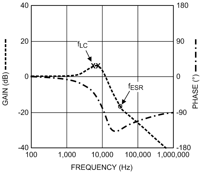
Figure 36 shows the bode plot of the above transfer function.
 Figure 36. Powertrain Bode Plot
The complex poles (fLC) created by the filter inductor and output capacitor cause a 180° phase shift as seen in Figure 36. The phase is boosted back up to -90° by virtue of the output capacitor ESR zero. The phase shift caused by the complex poles must be compensated to stabilize the loop response. The compensation network shown around the error amplifier in Figure 35 creates two poles, two zeros and a pole at the origin. Placing these poles and zeros at the correct frequencies optimizes the loop response. The compensator transfer function is:

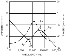
The pole located at the origin provides high DC gain to maximize DC load regulation performance. The other two poles and two zeros are strategically located to stabilize the voltage-mode loop depending on the power stage complex poles and damping characteristic, Q. Figure 37 illustrates a typical compensation transfer function.
 Figure 37. Type-lll Compensation Network Bode Plot
Km is the mid-band gain of the compensator and is estimated by:

fC is the desired crossover frequency and is normally selected between one tenth and one fifth of the switching frequency, fSW. The next set of equations show pole and zero locations expressed in terms of the components in the compensator feedback loop.

Depending on Q, the complex double pole causes an increase in gain at the LC resonant frequency and a precipitous drop in phase. To compensate for the phase drop, it is common practice to place both compensator zeros created by the Type-III compensation network at or slightly below the LC double pole frequency. The other two poles are located beyond this point. One pole is located at the zero caused by the output capacitor ESR and the other pole is placed at half the switching frequency to roll off the higher frequency response.

Conservative values for the compensation components are found by using the following equations.

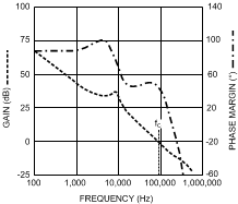
Once the compensation components are fixed, create a Bode plot of the loop response using all three transfer functions. Figure 38 provides an illustration of the loop response.
 Figure 38. Loop Response
It is important to always verify the stability by either observing the load transient response or by using a network analyzer. A phase margin between 45° and 70° is usually desired for voltage-mode controlled systems. Excessive phase margin causes slow system response to load transients whereas low phase margin is indicated by an oscillatory load transient response. If the peak voltage deviation is larger than desired, increase fC and recalculate the compensation components. If this amounts to a reduction in phase margin, the remaining option is to increase output capacitance.