ZHCS547K January 2010 – February 2018 LM27402
PRODUCTION DATA.
- 1 特性
- 2 应用
- 3 说明
- 4 修订历史记录
- 5 Pin Configuration and Functions
- 6 Specifications
-
7 Detailed Description
- 7.1 Overview
- 7.2 Functional Block Diagram
- 7.3
Feature Description
- 7.3.1 Wide Input Voltage Range
- 7.3.2 UVLO
- 7.3.3 Precision Enable
- 7.3.4 Soft-Start and Voltage Tracking
- 7.3.5 Output Voltage Setpoint and Accuracy
- 7.3.6 Voltage-Mode Control
- 7.3.7 Power Good
- 7.3.8 Inductor-DCR-Based Overcurrent Protection
- 7.3.9 Current Sensing
- 7.3.10 Power MOSFET Gate Drivers
- 7.3.11 Pre-Bias Start-up
- 7.4 Device Functional Modes
-
8 Application and Implementation
- 8.1
Application Information
- 8.1.1 Converter Design
- 8.1.2 Inductor Selection (L)
- 8.1.3 Output Capacitor Selection (COUT)
- 8.1.4 Input Capacitor Selection (CIN)
- 8.1.5 Using Precision Enable
- 8.1.6 Setting the Soft-Start Time
- 8.1.7 Tracking
- 8.1.8 Setting the Switching Frequency
- 8.1.9 Setting the Current Limit Threshold
- 8.1.10 Control Loop Compensation
- 8.1.11 MOSFET Gate Drivers
- 8.1.12 Power Loss and Efficiency Calculations
- 8.2 Typical Applications
- 8.1
Application Information
- 9 Power Supply Recommendations
- 10Layout
- 11器件和文档支持
- 12机械、封装和可订购信息
封装选项
机械数据 (封装 | 引脚)
散热焊盘机械数据 (封装 | 引脚)
订购信息
8.1.11 MOSFET Gate Drivers
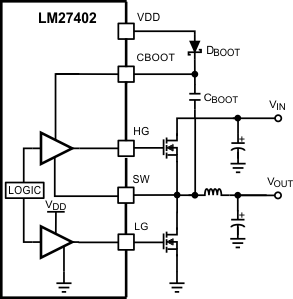
To drive large power MOSFETs with high gate charge, the LM27402 includes low impedance high-side and low-side gate drivers that source and sink high current for fast transition times and increased efficiency. The high-side gate driver is powered from a bootstrap circuit, whereas the low-side driver is powered by the VDD rail as shown in Figure 39.
 Figure 39. High-Side and Low-Side MOSFET Gate Drivers
The circuit in Figure 39 effectively supplies close to the VDD voltage (4.5 V) between the gate and the source of the high-side MOSFET during the on time. Use a Schottky diode for DBOOT with sufficient reverse voltage rating and continuous current rating. The average current through the boot diode depends on the gate charge of the high-side MOSFET and the switching frequency. It is calculated using Equation 24.

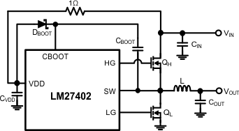
IDBOOT is the average current through the DBOOT diode, fSW is the switching frequency and QGHS is the gate charge of the high-side MOSFET. If the input voltage is below 5.5 V, it is recommended to connect VDD to the input supply of the LM27402 through a 1-Ω resistor as shown in Figure 40. This increases the gate voltage amplitude of both the low-side and high-side MOSFETs, thus reducing RDS(on).
 Figure 40. Tie VDD to VIN when VIN ≤ 5.5V