ZHCS547K January 2010 – February 2018 LM27402
PRODUCTION DATA.
- 1 特性
- 2 应用
- 3 说明
- 4 修订历史记录
- 5 Pin Configuration and Functions
- 6 Specifications
-
7 Detailed Description
- 7.1 Overview
- 7.2 Functional Block Diagram
- 7.3
Feature Description
- 7.3.1 Wide Input Voltage Range
- 7.3.2 UVLO
- 7.3.3 Precision Enable
- 7.3.4 Soft-Start and Voltage Tracking
- 7.3.5 Output Voltage Setpoint and Accuracy
- 7.3.6 Voltage-Mode Control
- 7.3.7 Power Good
- 7.3.8 Inductor-DCR-Based Overcurrent Protection
- 7.3.9 Current Sensing
- 7.3.10 Power MOSFET Gate Drivers
- 7.3.11 Pre-Bias Start-up
- 7.4 Device Functional Modes
-
8 Application and Implementation
- 8.1
Application Information
- 8.1.1 Converter Design
- 8.1.2 Inductor Selection (L)
- 8.1.3 Output Capacitor Selection (COUT)
- 8.1.4 Input Capacitor Selection (CIN)
- 8.1.5 Using Precision Enable
- 8.1.6 Setting the Soft-Start Time
- 8.1.7 Tracking
- 8.1.8 Setting the Switching Frequency
- 8.1.9 Setting the Current Limit Threshold
- 8.1.10 Control Loop Compensation
- 8.1.11 MOSFET Gate Drivers
- 8.1.12 Power Loss and Efficiency Calculations
- 8.2 Typical Applications
- 8.1
Application Information
- 9 Power Supply Recommendations
- 10Layout
- 11器件和文档支持
- 12机械、封装和可订购信息
封装选项
机械数据 (封装 | 引脚)
散热焊盘机械数据 (封装 | 引脚)
订购信息
5 Pin Configuration and Functions
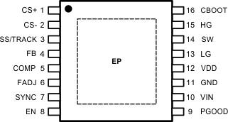
PWP Package
16-Pin HTSSOP
Top View

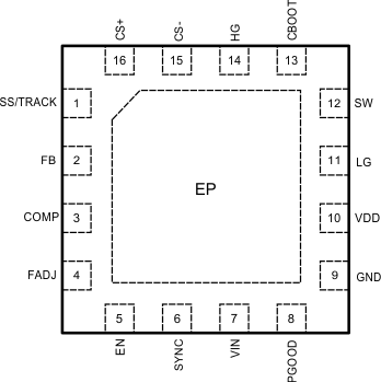
RUM Package
16-Pin WQFN
Top View

Pin Functions
| PIN | I/O(1) | DESCRIPTION | ||
|---|---|---|---|---|
| NAME | HTSSOP | WQFN | ||
| CBOOT | 16 | 13 | P | High-side gate driver supply rail. Connect a 100-nF ceramic capacitor from CBOOT to SW and a Schottky diode from VDD to CBOOT. |
| COMP | 5 | 3 | O | Output of the internal error amplifier. The COMP voltage is compared to an internally generated ramp at the PWM comparator to establish the duty cycle command. |
| CS+ | 1 | 16 | I | Current sense positive input. This pin is the noninverting input to the current-sense comparator. |
| CS– | 2 | 15 | I | Current sense negative input. This pin is the inverting input to the current-sense comparator. 10-µA of nominal offset current is provided for adjustable current limit setpoint. |
| EN | 8 | 5 | I | LM27402 enable pin. Apply a voltage typically higher than 1.17 V to EN and the LM27402 will begin to switch if VIN and VDD have exceeded their UVLO thresholds. A hysteresis of 100 mV on EN provides noise immunity. EN is internally tied to VDD through a 2-µA pullup current source. EN must not exceed the voltage on VDD. |
| FADJ | 6 | 4 | I | Frequency adjust input. The switching frequency is programmable between 200 kHz and 1.2 MHz by connecting a resistor between FADJ and GND. |
| FB | 4 | 2 | I | Feedback input. Inverting input to the error amplifier to set the output voltage and compensate the voltage-mode control loop. |
| GND | 11 | 9 | G | Common ground connection. This pin provides the power and signal return connections for analog functions, including low-side MOSFET gate return, soft-start capacitor, and frequency adjust resistor. |
| HG | 15 | 14 | O | High-side MOSFET gate drive output. |
| LG | 13 | 11 | O | Low-side MOSFET gate drive output. |
| PGOOD | 9 | 8 | O | Power Good monitor output. This open-drain output goes low during overcurrent, short-circuit, UVLO, output overvoltage and undervoltage, overtemperature, or when the output is not regulated (such as an output prebias). An external pullup resistor to VDD or to an external rail is required. Included is a 20-μs deglitch filter. The PGOOD voltage should not exceed 5.5 V. |
| SS/TRACK | 3 | 1 | I/O | Soft-start or tracking input. A start-up rate is defined with the use of an external soft-start capacitor from SS/TRACK to GND. A +3-µA current source charges the soft-start capacitor to set the output voltage rise time during start-up. SS/TRACK can also be controlled with an external voltage source for tracking applications. SS/TRACK voltage must not exceed the voltage on VDD. |
| SW | 14 | 12 | P | Power stage switch-node connection and return path for the high-side gate driver. |
| SYNC | 7 | 6 | I | Frequency synchronization input. Apply an external clock signal to SYNC to set the switching frequency. The SYNC frequency must be greater than the frequency set by the FADJ pin. If the signal is not present, the switching frequency will decrease to the frequency set by the FADJ resistor. SYNC must not exceed the voltage on VDD and must be tied to GND if not used. |
| VDD | 12 | 10 | P | Internal sub-regulated 4.5-V bias supply. VDD is used to supply the voltage on CBOOT to facilitate high-side MOSFET switching. Connect a 1-µF ceramic capacitor from VDD to GND as close as possible to the LM27402. VDD cannot be connected to a separate voltage rail. However, VDD can be connected to VIN to provide increased gate drive only if VIN ≤ 5.5 V. Use A 1-Ω, 1-µF input filter for increased noise rejection. |
| VIN | 10 | 7 | P | Input voltage supply rail with an operating range is 3 V to 20 V. This input is used to provide the feedforward modulation for output voltage control and for generating the internal bias supply voltage. Decouple VIN to GND locally with a 1-μF ceramic capacitor. For better noise rejection, connect to the power stage input rail with an RC filter. |
| EP | – | – | P | Exposed pad. Connect this pad to the PCB GND plane using multiple thermal vias. |
(1) P= Power, G = Ground, I = Input, O = Output