ZHCS547K January 2010 – February 2018 LM27402
PRODUCTION DATA.
- 1 特性
- 2 应用
- 3 说明
- 4 修订历史记录
- 5 Pin Configuration and Functions
- 6 Specifications
-
7 Detailed Description
- 7.1 Overview
- 7.2 Functional Block Diagram
- 7.3
Feature Description
- 7.3.1 Wide Input Voltage Range
- 7.3.2 UVLO
- 7.3.3 Precision Enable
- 7.3.4 Soft-Start and Voltage Tracking
- 7.3.5 Output Voltage Setpoint and Accuracy
- 7.3.6 Voltage-Mode Control
- 7.3.7 Power Good
- 7.3.8 Inductor-DCR-Based Overcurrent Protection
- 7.3.9 Current Sensing
- 7.3.10 Power MOSFET Gate Drivers
- 7.3.11 Pre-Bias Start-up
- 7.4 Device Functional Modes
-
8 Application and Implementation
- 8.1
Application Information
- 8.1.1 Converter Design
- 8.1.2 Inductor Selection (L)
- 8.1.3 Output Capacitor Selection (COUT)
- 8.1.4 Input Capacitor Selection (CIN)
- 8.1.5 Using Precision Enable
- 8.1.6 Setting the Soft-Start Time
- 8.1.7 Tracking
- 8.1.8 Setting the Switching Frequency
- 8.1.9 Setting the Current Limit Threshold
- 8.1.10 Control Loop Compensation
- 8.1.11 MOSFET Gate Drivers
- 8.1.12 Power Loss and Efficiency Calculations
- 8.2 Typical Applications
- 8.1
Application Information
- 9 Power Supply Recommendations
- 10Layout
- 11器件和文档支持
- 12机械、封装和可订购信息
封装选项
机械数据 (封装 | 引脚)
散热焊盘机械数据 (封装 | 引脚)
订购信息
10.1 Layout Guidelines
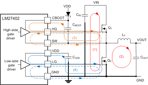
Careful PCB design and layout are important in a high current, fast switching circuit (with high current and voltage slew rates) to assure appropriate device operation and design robustness. As expected, certain issues must be considered before designing a PCB layout using the LM27402. The main switching loop of the power stage is denoted by 1 in Figure 48. The buck converter topology means that particularly high di/dt current will flow in loop 1, and it becomes mandatory to reduce the parasitic inductance of this loop by minimizing its effective loop area. For loop 2 however, the di/dt through inductor LF and capacitor COUT is naturally limited by the inductor. Keeping the area of loop 2 small is not nearly as important as that of loop 1. Also important are the gate drive loops of the low-side and high-side MOSFETs, denoted by 3 and 4, respectively, in Figure 48.
 Figure 48. DC/Dc Converter Ground System With Power Stage and Gate Drive Circuit Switching Loops