ZHCSDO1 May 2015 LM2775
PRODUCTION DATA.
- 1 特性
- 2 应用
- 3 说明
- 4 修订历史记录
- 5 Pin Configuration and Functions
- 6 Specifications
- 7 Detailed Description
- 8 Application and Implementation
- 9 Power Supply Recommendations
- 10Layout
- 11器件和文档支持
- 12机械、封装和可订购信息
8 Application and Implementation
NOTE
Information in the following applications sections is not part of the TI component specification, and TI does not warrant its accuracy or completeness. TI’s customers are responsible for determining suitability of components for their purposes. Customers should validate and test their design implementation to confirm system functionality.
8.1 Application Information
The LM2775 can create a 5-V system rail capable of delivering up to 200 mA of output current to the load. The 2-MHz switched capacitor boost allows for the use of small value discrete external components.
8.2 Typical Application
 Figure 19. Typical LM2775 Configuration
8.2.1 Design Requirements
| DESIGN PARAMETER | EXAMPLE VALUE |
|---|---|
| Input voltage range | 2.7 V to 5.5 V |
| Output current range | 0 mA to 200 mA (Max. current will depend on VIN) |
8.2.2 Detailed Design Procedure
8.2.2.1 Output Current Capability
The LM2775 provides 200 mA of output current when the input voltage is within 3.1 V to 5.5 V.
NOTE
Understanding relevant application issues is recommended and a thorough analysis of the application circuit should be performed when using the part outside operating ratings and/or specifications to ensure satisfactory circuit performance in the application. Special care should be paid to power dissipation and thermal effects. These parameters can have a dramatic impact on high-current applications, especially when the input voltage is high. (see the Power Dissipation section).
The schematic of Figure 20 is a simplified model of the LM2775 that is useful for evaluating output current capability. The model shows a linear pre-regulation block (Reg), a voltage doubler (2×), and an output resistance (ROUT). Output resistance models the output voltage droop that is inherent to switched capacitor converters. The output resistance of the LM2775 is 3.5 Ω (typical) and is approximately equal to twice the resistance of the four LM2775 switches. When the output voltage is in regulation, the regulator in the model controls the voltage V' to keep the output voltage equal to 5 V ± 4%. With increased output current, the voltage drop across ROUT increases. To prevent droop in output voltage, the voltage drop across the regulator is reduced, V' increases, and VOUT remains at 5 V. When the output current increases to the point that there is zero voltage drop across the regulator, V' equals the input voltage, and the output voltage is near the edge of regulation. Additional output current causes the output voltage to fall out of regulation, and the LM2775 operation is similar to a basic open-loop doubler. As in a voltage doubler, increase in output current results in output voltage drop proportional to the output resistance of the doubler. The out-of-regulation LM2775 output voltage can be approximated by:
Again, Equation 1 only applies at low input voltage and high output current where the LM2775 is not regulating. See Output Current vs. Output Voltage curves in the Typical Characteristics section for more details.
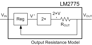 Figure 20. LM2775 Output Resistance Model
A more complete calculation of output resistance takes into account the effects of switching frequency, flying capacitance, and capacitor equivalent series resistance (ESR) (see Equation 2).

Switch resistance component (3 Ω typical) dominates the output resistance equation of the LM2775. With a 2-MHz typical switching frequency, the 1/(F×C) component of the output resistance contributes only 0.5 Ω to the total output resistance. Increasing the flying capacitance only provides minimal improvement to the total output current capability of the LM2775. In some applications it may be desirable to reduce the value of the flying capacitor below 1 µF to reduce solution size and/or cost, but this should be done with care so that output resistance does not increase to the point that undesired output voltage droop results. If ceramic capacitors are used, ESR will be a negligible factor in the total output resistance, as the ESR of quality ceramic capacitors is typically much less than 100 mΩ.
8.2.2.2 Efficiency
Charge-pump efficiency is derived in Equation 3 and Equation 4 (supply current and other losses are neglected for simplicity):
If one includes the quiescent current drawn by the LM2775 to operate, the following can be derived :

In Equation 3, G represents the charge pump gain. Efficiency is at its highest as G × VIN approaches VOUT. For the LM2775 device, G = 2.
8.2.2.3 Power Dissipation
LM2775 power dissipation (PD) is calculated simply by subtracting output power from input power:
Power dissipation increases with increased input voltage and output current, up to 1.35 W at the ends of the operating ratings (VIN = 5.5 V, IOUT = 200 mA). Internal power dissipation self-heats the device. Dissipating this amount power/heat so the LM2775 does not overheat is a demanding thermal requirement for a small surface-mount package. When soldered to a PCB with layout conducive to power dissipation, the excellent thermal properties of the WSON package enable this power to be dissipated from the LM2775 with little or no derating, even when the circuit is placed in elevated ambient temperatures.
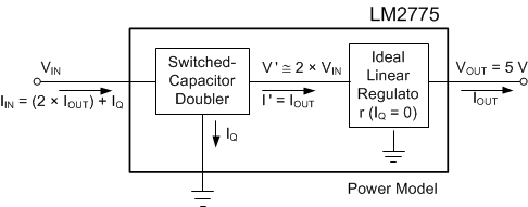 Figure 21. Power Model
8.2.2.4 Recommended Capacitor Types
The LM2775 requires 3 external capacitors for proper operation. Surface-mount multi-layer ceramic capacitors are recommended. These capacitors are small, inexpensive, and have very low ESR (≤ 15 mΩ typical). Tantalum capacitors, OS-CON capacitors, and aluminum electrolytic capacitors generally are not recommended for use with the LM2775 due to their high ESR compared to ceramic capacitors.
For most applications, ceramic capacitors with an X7R or X5R temperature characteristic are preferred for use with the LM2775. These capacitors have tight capacitance tolerance (as good as ±10%) and hold their value over temperature (X7R: ±15% over –55°C to 125°C; X5R: ±15% over –55°C to 85°C).
Capacitors with a Y5V or Z5U temperature characteristic are generally not recommended for use with the LM2775. These types of capacitors typically have wide capacitance tolerance (80% to 20%) and vary significantly over temperature (Y5V: 22%, –82% over –30°C to 85°C range; Z5U: 22%, –56% over 10°C to 85°C range). Under some conditions, a 1-µF-rated Y5V or Z5U capacitor could have a capacitance as low as 0.1 µF. Such detrimental deviation is likely to cause Y5V and Z5U capacitors to fail to meet the minimum capacitance requirements of the LM2775.
Net capacitance of a ceramic capacitor decreases with increased DC bias. This degradation can result in lower capacitance than expected on the input and/or output, resulting in higher ripple voltages and currents. Using capacitors at DC-bias voltages significantly below the capacitor voltage rating usually minimizes DC-bias effects. Consult capacitor manufacturers for information on capacitor DC-bias characteristics.
Capacitance characteristics can vary quite dramatically with different application conditions, capacitor types, and capacitor manufacturers. It is strongly recommended that the LM2775 circuit be thoroughly evaluated early in the design-in process with the mass-production capacitors of choice. This helps ensure that any such variability in capacitance does not negatively impact circuit performance.
The voltage rating of the output capacitor should be 10 V or more. All other capacitors should have a voltage rating at or above the maximum input voltage of the application.
8.2.2.5 Output Capacitor and Output Voltage Ripple
The output capacitor in the LM2775 circuit (COUT) directly impacts the magnitude of output voltage ripple. Other prominent factors also affecting output voltage ripple include input voltage, output current, and flying capacitance. One important generalization can be made: increasing (decreasing) the output capacitance results in a proportional decrease (increase) in output voltage ripple. A simple approximation of output ripple is determined by calculating the amount of voltage droop that occurs when the output of the LM2775 is not being driven. This occurs during the charge phase (φ1). During this time, the load is driven solely by the charge on the output capacitor. The magnitude of the ripple thus follows the basic discharge equation for a capacitor (I = C × dV/dt), where discharge time is one-half the switching period, or 0.5/FSW (see Equation 6).

A more thorough and accurate examination of factors that affect ripple requires including effects of phase non-overlap times and output capacitor ESR. In order for the LM2775 to operate properly, the two phases of operation must never coincide. (If this were to happen all switches would be closed simultaneously, shorting input, output, and ground). Thus, non-overlap time is built into the clocks that control the phases. Since the output is not being driven during the non-overlap time, this time should be accounted for in calculating ripple. Actual output capacitor discharge time is approximately 60% of a switching period, or 0.6/FSW (see Equation 7).

NOTE
In typical high-current applications, a 10-µF, 10-V low-ESR ceramic output capacitor is recommended. Different output capacitance values can be used to reduce ripple, shrink the solution size, and/or cut the cost of the solution. But changing the output capacitor may also require changing the flying capacitor and/or input capacitor to maintain good overall circuit performance. If a small output capacitor is used and PFM mode is enabled, the output ripple can become large during the transition between PFM mode and constant switching. To prevent toggling, a 2-µF capacitance is recommended. For example, a 10-µF, 10-V output capacitor in a 0402 case size will typically only have 2-µF capacitance when biased to 5 V.
High ESR in the output capacitor increases output voltage ripple. If a ceramic capacitor is used at the output, this is usually not a concern because the ESR of a ceramic capacitor is typically very low and has only a minimal impact on ripple magnitudes. If a different capacitor type with higher ESR is used (tantalum, for example), the ESR could result in high ripple. To eliminate this effect, the net output ESR can be significantly reduced by placing a low-ESR ceramic capacitor in parallel with the primary output capacitor. The low ESR of the ceramic capacitor is in parallel with the higher ESR, resulting in a low net ESR based on the principles of parallel resistance reduction.
8.2.2.6 Input Capacitor and Input Voltage Ripple
The input capacitor (CIN) is a reservoir of charge that aids a quick transfer of charge from the supply to the flying capacitor during the charge phase of operation. The input capacitor helps to keep the input voltage from drooping at the start of the charge phase when the flying capacitor is connected to the input. It also filters noise on the input pin, keeping this noise out of sensitive internal analog circuitry that is biased off the input line.
Much like the relationship between the output capacitance and output voltage ripple, input capacitance has a dominant and first-order effect on input ripple magnitude. Increasing (decreasing) the input capacitance results in a proportional decrease (increase) in input voltage ripple. Input voltage, output current, and flying capacitance also affect input ripple levels to some degree.
In typical high-current applications, a 10-µF low-ESR ceramic capacitor is recommended on the input. Different input capacitance values can be used to reduce ripple, shrink the solution size, and/or cut the cost of the solution. But changing the input capacitor may also require changing the flying capacitor and/or output capacitor to maintain good overall circuit performance.
8.2.2.7 Flying Capacitor
The flying capacitor (C1) transfers charge from the input to the output. Flying capacitance can impact both output current capability and ripple magnitudes. If flying capacitance is too small, the LM2775 may not be able to regulate the output voltage when load currents are high. On the other hand, if the flying capacitance is too large, the flying capacitor might overwhelm the input and output capacitors, resulting in increased input and output ripple.
In typical high-current applications, 1-µF low-ESR ceramic capacitors are recommended for the flying capacitor. Polarized capacitors (tantalum, aluminum electrolytic, etc.) must not be used for the flying capacitor, as they could become reverse-biased during LM2775 operation.
8.2.3 Application Curve
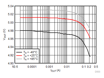
| VIN = 3.3 V | PFM = '0' | |
8.2.4 USB OTG / Mobile HDMI Power Supply
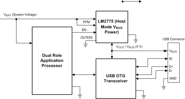 Figure 23. USB OTG Configuration
8.2.4.1 Design Requirements
| DESIGN PARAMETER | EXAMPLE VALUE |
|---|---|
| Input voltage range | 2.7 V to 5.5 V |
| Output current range | 0 mA to 200 mA (Max. current will depend on VIN) |
8.2.4.2 Detailed Design Procedure
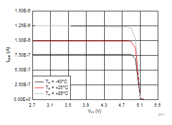
The 5-V output mode is normally used for the USB OTG / Mobile HDMI application. Therefore, the LM2775 can be enabled/disabled by applying a logic signal on only the EN pin while grounding the OUTDIS pin. Depending on the USB/HDMI mode of the application, the LM2775 can be enabled to drive the power bus line (Host), or disabled to put its output in high impedance allowing an external supply to drive the bus line (Slave). In addition to the high impedance-backdrive protection, the output current limit protection is 250 mA (typical), well within the USB OTG and HDMI requirements.
8.2.4.3 Application Curve
| EN = '0' | OUTDIS = '0' | |