ZHCSDP4B May 2015 – February 2017 LM2776
PRODUCTION DATA.
8 Application and Implementation
NOTE
Information in the following applications sections is not part of the TI component specification, and TI does not warrant its accuracy or completeness. TI’s customers are responsible for determining suitability of components for their purposes. Customers should validate and test their design implementation to confirm system functionality.
8.1 Application Information
The LM2776 CMOS charge-pump voltage converter inverts a positive voltage in the range of 2.7 V to 5.5 V to the corresponding negative voltage of −2.7 V to −5.5 V. The device uses three low-cost capacitors to provide up to 200 mA of output current. The LM2776 operates at 2-MHz oscillator frequency to reduce output resistance and voltage ripple under heavy loads. With an operating current of only 100 µA (operating efficiency greater than 91% with most loads) and 1-µA typical shutdown current, the LM2776 provides ideal performance for battery-powered systems.
8.2 Typical Application - Voltage Inverter
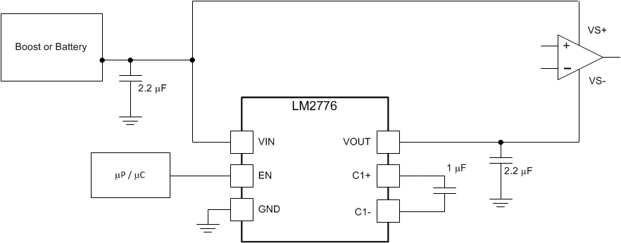
 Figure 18. Voltage Inverter
8.2.1 Design Requirements
Example requirements for typical voltage inverter applications:
| DESIGN PARAMETER | EXAMPLE VALUE |
|---|---|
| Input voltage range | 2.7 V to 5.5 V |
| Output current | 0 mA to 200 mA |
| Boost switching frequency | 2 MHz |
8.2.2 Detailed Design Requirements
The main application of LM2776 is to generate a negative supply voltage. The voltage inverter circuit uses only three external capacitors with an range of the input supply voltage from 2.7 V to 5.5 V.
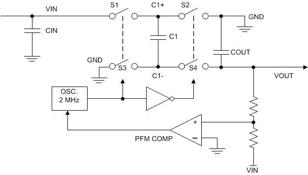
The LM2776 contains four large CMOS switches which are switched in a sequence to invert the input supply voltage. Energy transfer and storage are provided by external capacitors. Figure 19 shows the voltage conversion scheme. When S1 and S3 are closed, C1 charges to the supply voltage VIN. During this time interval, switches S2 and S4 are open. In the second time interval, S1 and S3 are open; at the same time, S2 and S4 are closed, C1 is charging C2. After a number of cycles, the voltage across C2 is pumped to VIN. Because the anode of C2 is connected to ground, the output at the cathode of C2 equals −(VIN) when there is no load current. The output voltage drop when a load is added is determined by the parasitic resistance (Rds(on) of the MOSFET switches and the equivalent series resistance (ESR) of the capacitors) and the charge transfer loss between capacitors.
 Figure 19. Voltage Inverting Principle
The output characteristics of this circuit can be approximated by an ideal voltage source in series with a resistance. The voltage source equals − (VIN). The output resistance ROUT is a function of the ON resistance of the internal MOSFET switches, the oscillator frequency, the capacitance and ESR of C1 and C2. Because the switching current charging and discharging C1 is approximately twice as the output current, the effect of the ESR of the pumping capacitor C1 is multiplied by four in the output resistance. The output capacitor C2 is charging and discharging at a current approximately equal to the output current, therefore, its ESR only counts once in the output resistance. A good approximation of ROUT is:
where
- RSW is the sum of the ON resistance of the internal MOSFET switches shown in Figure 19.
High-capacitance, low-ESR ceramic capacitors reduce the output resistance.
8.2.2.1 Efficiency
Charge-pump efficiency is defined as
where
- IQ (VIN) is the quiescent power loss of the device.
8.2.2.2 Power Dissipation
LM2776 power dissipation (PD) is calculated simply by subtracting output power from input power:
Power dissipation increases with increased input voltage and output current. Internal power dissipation self-heats the device. Dissipating this amount power/heat so the LM2776 does not overheat is a demanding thermal requirement for a small surface-mount package. When soldered to a PCB with layout conducive to power dissipation, the thermal properties of the SOT package enable this power to be dissipated from the LM2776 with little or no derating, even when the circuit is placed in elevated ambient temperatures when the output current is 200 mA or less.
8.2.2.3 Capacitor Selection
The LM2776 requires 3 external capacitors for proper operation. TI recommends urface-mount multi-layer ceramic capacitors. These capacitors are small, inexpensive, and have very low ESR (≤ 15 mΩ typical). Tantalum capacitors, OS-CON capacitors, and aluminum electrolytic capacitors generally are not recommended for use with the LM2776 due to their high ESR, as compared to ceramic capacitors.
For most applications, ceramic capacitors with an X7R or X5R temperature characteristic are preferred for use with the LM2776. These capacitors have tight capacitance tolerance (as good as ±10%) and hold their value over temperature (X7R: ±15% over –55ºC to 125°C; X5R: ±15% over –55°C to 85°C).
Capacitors with a Y5V or Z5U temperature characteristic are generally not recommended for use with the LM2776. These types of capacitors typically have wide capacitance tolerance (80%, …20%) and vary significantly over temperature (Y5V: 22%, –82% over –30°C to 85°C range; Z5U: 22%, –56% over 10°C to 85°C range). Under some conditions, a 1-µF-rated Y5V or Z5U capacitor could have a capacitance as low as 0.1 µF. Such detrimental deviation is likely to cause Y5V and Z5U capacitors to fail to meet the minimum capacitance requirements of the LM2776.
Net capacitance of a ceramic capacitor decreases with increased DC bias. This degradation can result in lower capacitance than expected on the input and/or output, resulting in higher ripple voltages and currents. Using capacitors at DC bias voltages significantly below the capacitor voltage rating usually minimizes DC bias effects. Consult capacitor manufacturers for information on capacitor DC bias characteristics.
Capacitance characteristics can vary quite dramatically with different application conditions, capacitor types, and capacitor manufacturers. It is strongly recommended that the LM2776 circuit be thoroughly evaluated early in the design-in process with the mass-production capacitors of choice. This helps ensure that any such variability in capacitance does not negatively impact circuit performance.
The voltage rating of the output capacitor must be 10 V or more. For example, a 10-V 0603 1-µF is acceptable for use with the LM2776, as long as the capacitance does not fall below a minimum of 0.5 µF in the intended application. All other capacitors must have a voltage rating at or above the maximum input voltage of the application. Select the capacitors such that the capacitance on the input does not fall below 0.7 µF, and the capacitance of the flying capacitor does not fall below 0.2 µF.
8.2.2.4 Output Capacitor and Output Voltage Ripple
The peak-to-peak output voltage ripple is determined by the oscillator frequency, the capacitance and ESR of the output capacitor COUT:
In typical applications, a 1-µF low-ESR ceramic output capacitor is recommended. Different output capacitance values can be used to reduce ripple shrink the solution size, and/or cut the cost of the solution. But changing the output capacitor may also require changing the flying capacitor and/or input capacitor to maintain good overall circuit performance.
NOTE
In high-current applications, TI recommends a 10-µF, 10-V low-ESR ceramic output capacitor. If a small output capacitor is used, the output ripple can become large during the transition between PFM mode and constant switching. To prevent toggling, a 2-µF capacitance is recommended. For example, a 10- µF, 10-V output capacitor in a 0402 case size typically only has 2-µF capacitance when biased to 5 V.
High ESR in the output capacitor increases output voltage ripple. If a ceramic capacitor is used at the output, this is usually not a concern because the ESR of a ceramic capacitor is typically very low and has only a minimal impact on ripple magnitudes. If a different capacitor type with higher ESR is used (tantalum, for example), the ESR could result in high ripple. To eliminate this effect, the net output ESR can be significantly reduced by placing a low-ESR ceramic capacitor in parallel with the primary output capacitor. The low ESR of the ceramic capacitor is in parallel with the higher ESR, resulting in a low net ESR based on the principles of parallel resistance reduction.
8.2.2.5 Input Capacitor
The input capacitor (CIN) is a reservoir of charge that aids a quick transfer of charge from the supply to the flying capacitors during the charge phase of operation. The input capacitor helps to keep the input voltage from drooping at the start of the charge phase when the flying capacitors are connected to the input. It also filters noise on the input pin, keeping this noise out of sensitive internal analog circuitry that is biased off the input line.
Much like the relationship between the output capacitance and output voltage ripple, input capacitance has a dominant and first-order effect on input ripple magnitude. Increasing (decreasing) the input capacitance results in a proportional decrease (increase) in input voltage ripple. Input voltage, output current, and flying capacitance also affects input ripple levels to some degree.
In typical applications, a 1-µF low-ESR ceramic capacitor is recommended on the input. When operating near the maximum load of 200 mA, a minimum recommended input capacitance after taking into the DC-bias derating is 2 µF or larger. Different input capacitance values can be used to reduce ripple, shrink the solution size, and/or cut the cost of the solution.
8.2.2.6 Flying Capacitor
The flying capacitor (C1) transfers charge from the input to the output. Flying capacitance can impact both output current capability and ripple magnitudes. If flying capacitance is too small, the LM2776 may not be able to regulate the output voltage when load currents are high. On the other hand, if the flying capacitance is too large, the flying capacitor might overwhelm the input and output capacitors, resulting in increased input and output ripple.
In typical high-current applications, TI recommends 0.47-µF or 1-µF 10 V low-ESR ceramic capacitors for the flying capacitors. Polarized capacitors (tantalum, aluminum electrolytic, etc.) must not be used for the flying capacitor, as they could become reverse-biased during LM2776 operation.
8.2.3 Application Curve
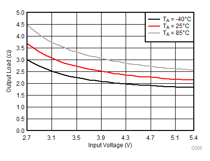
 Figure 20. Output Impedance vs Input Voltage