ZHCSEO7C October 2015 – January 2017 LM27761
PRODUCTION DATA.
- 1 特性
- 2 应用
- 3 说明
- 4 修订历史记录
- 5 Pin Configuration and Functions
- 6 Specifications
- 7 Detailed Description
-
8 Application and Implementation
- 8.1 Application Information
- 8.2
Typical Application - Regulated Voltage Inverter
- 8.2.1 Design Requirements
- 8.2.2 Detailed Design Procedure
- 8.2.3 Application Curves
- 9 Power Supply Recommendations
- 10Layout
- 11器件和文档支持
- 12机械、封装和可订购信息
7 Detailed Description
7.1 Overview
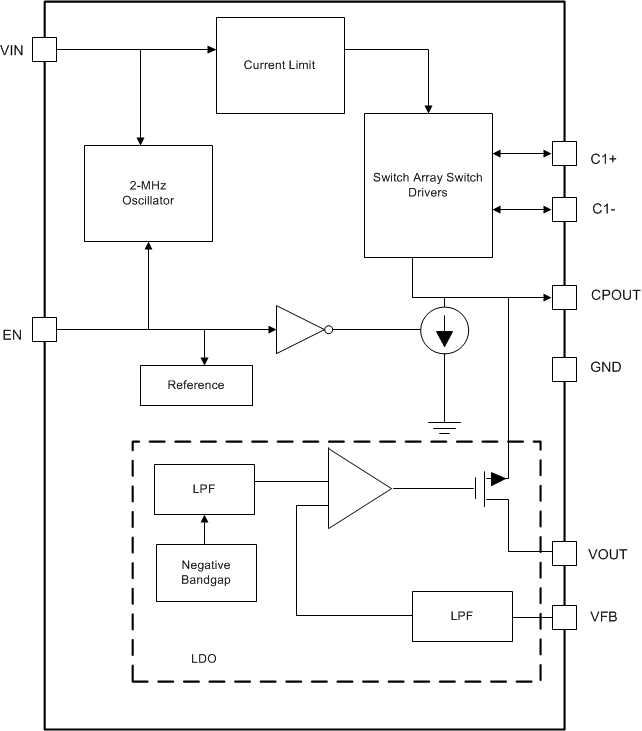
The LM27761 regulated charge-pump voltage converter inverts a positive voltage in the range of 2.7 V to 5.5 V to a negative voltage in the range of –1.5 V to –5 V. The negative LDO (low drop-out regulator), at the output of the charge-pump voltage converter, allows the device to provide a very low noise output, low output-voltage ripple, high PSRR, and low line and load transient responses. The output is externally configurable with gain-setting resistors. The LM27761 uses four low-cost capacitors to deliver up to 250 mA of output current.
7.2 Functional Block Diagram

7.3 Feature Description
7.3.1 Undervoltage Lockout
The LM27761 has an internal comparator that monitors the voltage at VIN and forces the device into shutdown if the input voltage drops to 2.4 V. If the input voltage rises above 2.6 V, the LM27761 resumes normal operation.
7.3.2 Input Current Limit
The LM27761 contains current limit circuitry that protects the device in the event of excessive input current and/or output shorts to ground. The input current is limited to 500 mA (typical) when the output is shorted directly to ground. When the LM27761 is current limiting, power dissipation in the device is likely to be quite high. In this event, thermal cycling is expected.
7.3.3 PFM Operation
To minimize quiescent current during light load operation, the LM27761 allows PFM or pulse-skipping operation. By allowing the charge pump to switch less when the output current is low, the quiescent current drawn from the power source is minimized. The frequency of pulsed operation is not limited and can drop into the sub-2-kHz range when unloaded. As the load increases, the frequency of pulsing increases until it transitions to constant frequency. The fundamental switching frequency in the LM27761 is 2 MHz.
7.3.4 Output Discharge
In shutdown, the LM27761 actively pulls down on the output of the device until the output voltage reaches GND. In this mode, the current drawn from the output is approximately 1.85 mA.
7.3.5 Thermal Shutdown
The LM27761 implements a thermal shutdown mechanism to protect the device from damage due to overheating. When the junction temperature rises to 150°C (typical), the device switches into shutdown mode. The LM27761 releases thermal shutdown when the junction temperature is reduced to 130°C (typical).
Thermal shutdown is most often triggered by self-heating, which occurs when there is excessive power dissipation in the device and/or insufficient thermal dissipation. The LM27761 device power dissipation increases with increased output current and input voltage. When self-heating brings on thermal shutdown, thermal cycling is the typical result. Thermal cycling is the repeating process where the part self-heats, enters thermal shutdown (where internal power dissipation is practically zero), cools, turns on, and then heats up again to the thermal shutdown threshold. Thermal cycling is recognized by a pulsing output voltage and can be stopped by reducing the internal power dissipation (reduce input voltage and/or output current) or the ambient temperature. If thermal cycling occurs under desired operating conditions, thermal dissipation performance must be improved to accommodate the power dissipation of the device.
7.4 Device Functional Modes
7.4.1 Shutdown Mode
An enable pin (EN) pin is available to disable the device and place the LM27761 into shutdown mode reducing the quiescent current to 7 µA. In shutdown, the output of the LM27761 is pulled to ground by an internal pullup current source (approximately 1.85 mA).
7.4.2 Enable Mode
Applying a voltage greater than 1.2 V to the EN pin brings the device into enable mode. When unloaded, the input current during operation is 370 µA. As the load current increases, so does the quiescent current. When enabled, the output voltage is equal to the inverse of the input voltage minus the voltage drop across the charge pump.