ZHCSEO7C October 2015 – January 2017 LM27761
PRODUCTION DATA.
- 1 特性
- 2 应用
- 3 说明
- 4 修订历史记录
- 5 Pin Configuration and Functions
- 6 Specifications
- 7 Detailed Description
-
8 Application and Implementation
- 8.1 Application Information
- 8.2
Typical Application - Regulated Voltage Inverter
- 8.2.1 Design Requirements
- 8.2.2 Detailed Design Procedure
- 8.2.3 Application Curves
- 9 Power Supply Recommendations
- 10Layout
- 11器件和文档支持
- 12机械、封装和可订购信息
8 Application and Implementation
NOTE
Information in the following applications sections is not part of the TI component specification, and TI does not warrant its accuracy or completeness. TI’s customers are responsible for determining suitability of components for their purposes. Customers should validate and test their design implementation to confirm system functionality.
8.1 Application Information
The LM27761 low-noise charge-pump voltage converter inverts a positive voltage in the range of 2.7 V to 5.5 V to a negative output voltage configurable with external gain setting resistors. The device uses four low-cost capacitors to provide up to 250 mA of output current. The LM27761 operates at a 2-MHz oscillator frequency to reduce charge-pump output resistance and voltage ripple under heavy loads. With an operating current of only 370 µA and 7-µA typical shutdown current, the LM27761 provides ideal performance for battery-powered systems.
8.2 Typical Application - Regulated Voltage Inverter
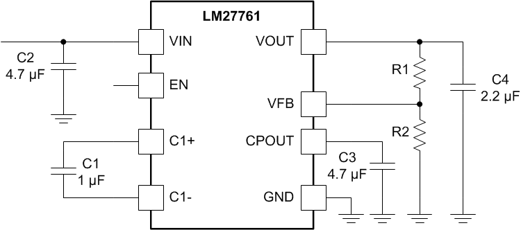 Figure 16. LM27761 Typical Application
8.2.1 Design Requirements
Example requirements for typical applications using the LM27761 device are listed in Table 1:
Table 1. Design Parameters
| DESIGN PARAMETER | EXAMPLE VALUE |
|---|---|
| Input voltage | 2.7 V to 5.5 V |
| Output voltage | –1.5 V to –5 V |
| Output current | 0 mA to 250 mA |
| Boost switching frequency | 2 MHz |
8.2.2 Detailed Design Procedure
8.2.2.1 Custom Design With WEBENCH® Tools
Click here to create a custom design using the LM27761 device with the WEBENCH® Power Designer.
- Start by entering the input voltage (VIN), output voltage (VOUT), and output current (IOUT) requirements.
- Optimize the design for key parameters such as efficiency, footprint, and cost using the optimizer dial.
- Compare the generated design with other possible solutions from Texas Instruments.
The WEBENCH Power Designer provides a customized schematic along with a list of materials with real-time pricing and component availability.
In most cases, these actions are available:
- Run electrical simulations to see important waveforms and circuit performance
- Run thermal simulations to understand board thermal performance
- Export customized schematic and layout into popular CAD formats
- Print PDF reports for the design, and share the design with colleagues
Get more information about WEBENCH tools at www.ti.com/WEBENCH.
8.2.2.2 Charge-Pump Voltage Inverter
The main application of the LM27761 is to generate a regulated negative supply voltage. The voltage inverter circuit uses only three external capacitors, and the LDO regulator circuit uses one additional output capacitor.
The voltage inverter portion of the LM27761 contains four large CMOS switches which are switched in sequence to invert the input supply voltage. Energy transfer and storage are provided by external capacitors. Figure 17 shows the voltage switches S2 and S4 are open. In the second time interval, S1 and S3 are open; at the same time, S2 and S4 are closed, and C1 is charging C3. After a number of cycles, the voltage across C3 is pumped into VIN. Because the anode of C3 is connected to ground, the output at the cathode of C3 equals –(VIN) when there is no load current. When a load is added the output voltage dropis determined by the parasitic resistance (RDSON of the MOSFET switches and the equivalent series resistance (ESR) of the capacitors) and the charge transfer loss between the capacitors.
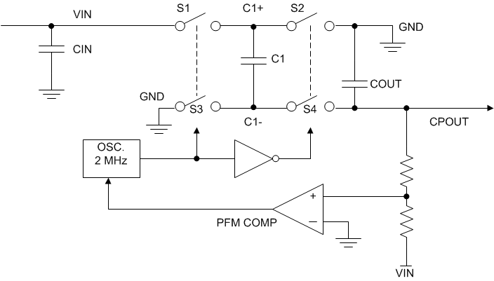 Figure 17. Voltage Inverting Principle
The output characteristic of this circuit can be approximated by an ideal voltage source in series with a resistance. The voltage source equals –(VIN). The output resistance ROUT is a function of the ON resistance of the internal MOSFET switches, the oscillator frequency, the capacitance, and the ESR of C1 and C3. Because the switching current charging and discharging C1 is approximately twice as the output current, the effect of the ESR of the pumping capacitor C1 is multiplied by four in the output resistance. The charge-pump output capacitor C3 is charging and discharging at a current approximately equal to the output current; therefore, its ESR only counts once in the output resistance. A good approximation of charge-pump ROUT is shown in Equation 1:
where
- RSW is the sum of the ON resistance of the internal MOSFET switches shown in Figure 17.
High capacitance and low-ESR ceramic capacitors reduce the output resistance.
8.2.2.3 Negative Low-Dropout Linear Regulator
At the output of the inverting charge-pump the LM27761 features a low-dropout, linear negative voltage regulator (LDO). The LDO output is rated for a current of 250 mA. This negative LDO allows the device to provide a very low noise output, low output voltage ripple, high PSRR, and low line or load transient response.
8.2.2.4 Power Dissipation
The allowed power dissipation for any package is a measure of the ability of the device to pass heat from the junctions of the device to the heatsink and the ambient environment. Thus, the power dissipation is dependent on the ambient temperature and the thermal resistance across the various interfaces between the die junction and ambient air.
The maximum allowable power dissipation can be calculated by Equation 2:
The actual power being dissipated in the device can be represented by Equation 3:
Equation 2 and Equation 3 establish the relationship between the maximum power dissipation allowed due to thermal consideration, the voltage drop across the device, and the continuous current capability of the device. These equations must be used to determine the optimum operating conditions for the device in a given application.
In lower power dissipation applications the maximum ambient temperature (TA-MAX) may be increased. In higher power dissipation applications the maximum ambient temperature(TA-MAX) may have to be derated. TA-MAX can be calculated using Equation 4:
where
- TJ-MAX-OP = maximum operating junction temperature (125°C)
- PD-MAX = the maximum allowable power dissipation
- RθJA = junction-to-ambient thermal resistance of the package
Alternately, if TA-MAX cannot be derated, the power dissipation value must be reduced. This can be accomplished by reducing the input voltage as long as the minimum VIN is not violated, or by reducing the output current, or some combination of the two.
8.2.2.5 Output Voltage Setting
The output voltage of the LM27761 is externally configurable. The value of R1 and R2 determines the output voltage setting. The output voltage can be calculated using Equation 5:
8.2.2.6 External Capacitor Selection
The LM27761 requires 4 external capacitors for proper operation. Surface-mount multi-layer ceramic capacitors are recommended. These capacitors are small, inexpensive, and have very low ESR (≤ 15 mΩ typical). Tantalum capacitors, OS-CON capacitors, and aluminum electrolytic capacitors generally are not recommended for use with the LM27761 due to their high ESR compared to ceramic capacitors.
For most applications, ceramic capacitors with an X7R or X5R temperature characteristic are preferable for use with the LM27761. These capacitors have tight capacitance tolerances (as good as ±10%) and hold their value over temperature (X7R: ±15% over –55°C to +125°C; X5R ±15% over –55°C to +85°C).
Using capacitors with a Y5V or Z5U temperature characteristic is generally not recommended for the LM27761. These capacitors typically have wide capacitance tolerance (80%, ….20%) and vary significantly over temperature (Y5V: 22%, –82% over –30°C to +85°C range; Z5U: 22%, –56% over 10°C to 85°C range). Under some conditions a 1-µF-rated Y5V or Z5U capacitor could have a capacitance as low as 0.1 µF. Such detrimental deviation is likely to cause Y5V and Z5U capacitors to fail to meet the minimum capacitance requirements of the LM27761.
Net capacitance of a ceramic capacitor decreases with increased DC bias. This degradation can result in lower-than-expected capacitance on the input and/or output, resulting in higher ripple voltages and currents. Using capacitors at DC bias voltages significantly below the capacitor voltage rating usually minimizes DC bias effects. Consult capacitor manufacturers for information on capacitor DC bias characteristics.
Capacitance characteristics can vary quite dramatically with different application conditions, capacitor types, and capacitor manufacturers. TI strongly recommends that the LM27761 circuit be evaluated thoroughly early in the design-in process with the mass-production capacitor of choice. This helps ensure that any such variability in capacitance does not negatively impact circuit performance.
8.2.2.6.1 Charge-Pump Output Capacitor
In typical applications, a 4.7-µF low-ESR ceramic charge-pump output capacitor (C3) is recommended. Different output capacitance values can be used to reduce charge pump ripple, shrink the solution size, and/or cut the cost of the solution. However, changing the output capacitor may also require changing the flying capacitor or input capacitor to maintain good overall circuit performance.
In higher-current applications, a 10-µF, 10-V low-ESR ceramic output capacitor is recommended. If a small output capacitor is used, the output ripple can become large during the transition between PFM mode and constant switching. To prevent toggling, a 2-µF capacitance is recommended. For example, 10-µF, 10-V output capacitor in a 0402 case size typically has only 2-µF capacitance when biased to 5 V.
8.2.2.6.2 Input Capacitor
The input capacitor (C2) is a reservoir of charge that aids in a quick transfer of charge from the supply to the flying capacitors during the charge phase of operation. The input capacitor helps to keep the input voltage from drooping at the start of the charge phase when the flying capacitors are connected to the input. It also filters noise on the input pin, keeping this noise out of the sensitive internal analog circuitry that is biased off the input line.
Input capacitance has a dominant and first-order effect on the input ripple magnitude. Increasing (decreasing) the input capacitance results in a proportional decrease (increase) in input voltage ripple. Input voltage, output current, and flying capacitance also affects input ripple levels to some degree.
In typical applications, a 4.7-µF low-ESR ceramic capacitor is recommended on the input. When operating near the maximum load of 250 mA, after taking into the DC bias derating, a minimum recommended input capacitance is 2 µF or larger. Different input capacitance values can be used to reduce ripple, shrink the solution size, and/or cut the cost of the solution.
8.2.2.6.3 Flying Capacitor
The flying capacitor (C1) transfers charge from the input to the output. Flying capacitance can impact both output current capability and ripple magnitudes. If flying capacitance is too small, the LM27761 may not be able to regulate the output voltage when load currents are high. On the other hand, if the flying capacitance is too large, the flying capacitor might overwhelm the input and charge pump output capacitors, resulting in increased input and output ripple.
In typical high-current applications, 0.47-µF or 1-µF 10-V low-ESR ceramic capacitors are recommended for the flying capacitors. Polarized capacitors (tantalum, aluminum, electrolytic, etc.) must not be used for the flying capacitor, as they could become reverse-biased during LM27761 operation.
8.2.2.6.4 LDO Output Capacitor
The LDO output capacitor (C4) value and the ESR affect stability, output ripple, output noise, PSRR and transient response. The LM27761 only requires the use of a 2.2-µF ceramic output capacitor for stable operation. For typical applications, a 2.2-µF ceramic output capacitor located close to the output is sufficient.
8.2.3 Application Curves
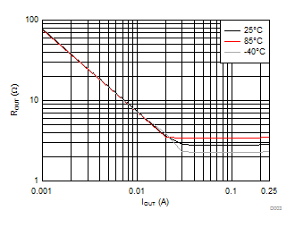
| VIN = 3 V | VOUT = –1.8 V |
Output Current
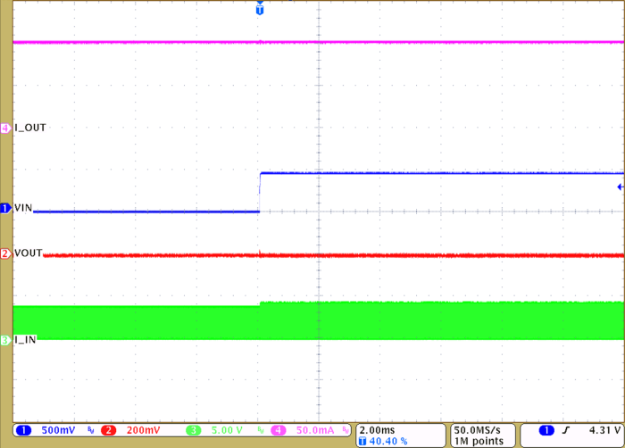
| VIN = 4V to 4.5 V | VOUT = –1.8 V | IOUT = 100 mA |
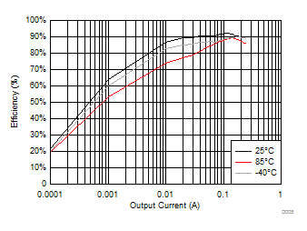
| VIN = 5.5 V | VOUT = –5 V | R1 = 1.54 MΩ | R2 = 500 kΩ | |
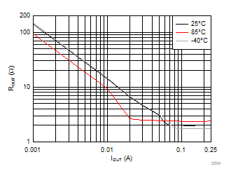
| VIN = 5.5 V | VOUT = –5 V |
Output Current
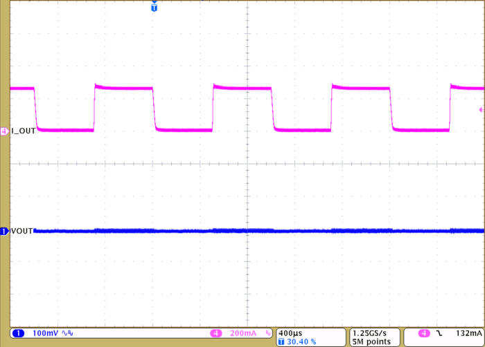
| VIN = 3 V | VOUT = –1.8 V |