ZHCSOW0J January 2000 – March 2022 LM158-N , LM258-N , LM2904-N , LM358-N
PRODUCTION DATA
- 1 特性
- 2 应用
- 3 说明
- 4 Revision History
- 5 Pin Configuration and Functions
- 6 Specifications
- 7 Detailed Description
- 8 Application and Implementation
- 9 Power Supply Recommendations
- 10Layout
- 11Device and Documentation Support
- 12Mechanical, Packaging, and Orderable Information
封装选项
机械数据 (封装 | 引脚)
散热焊盘机械数据 (封装 | 引脚)
订购信息
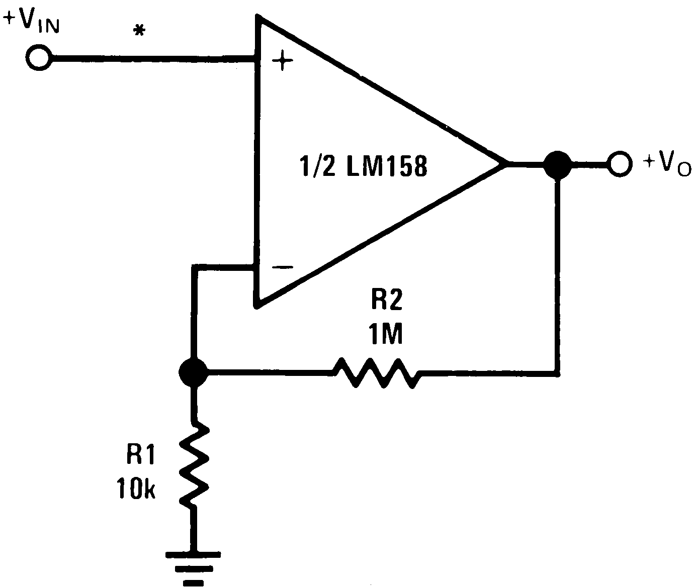
8.2.1 Noninverting DC Gain
Figure 8-1 shows a high input impedance non-inverting circuit. This circuit gives a closed-loop gain equal to the ratio of the sum of R1 and R2 to R1 and a closed-loop 3 dB bandwidth equal to the amplifier unity-gain frequency divided by the closed-loop gain. This design has the benefit of a very high input impedance, which is equal to the differential input impedance multiplied by loop gain. (Open loop gain/Closed loop gain.) In DC coupled applications, input impedance is not as important as input current and its voltage drop across the source resistance. Note that the amplifier output will go into saturation if the input is allowed to float. This may be important if the amplifier must be switched from source to source.
