ZHCS531G September 2007 – January 2018 LM3103
PRODUCTION DATA.
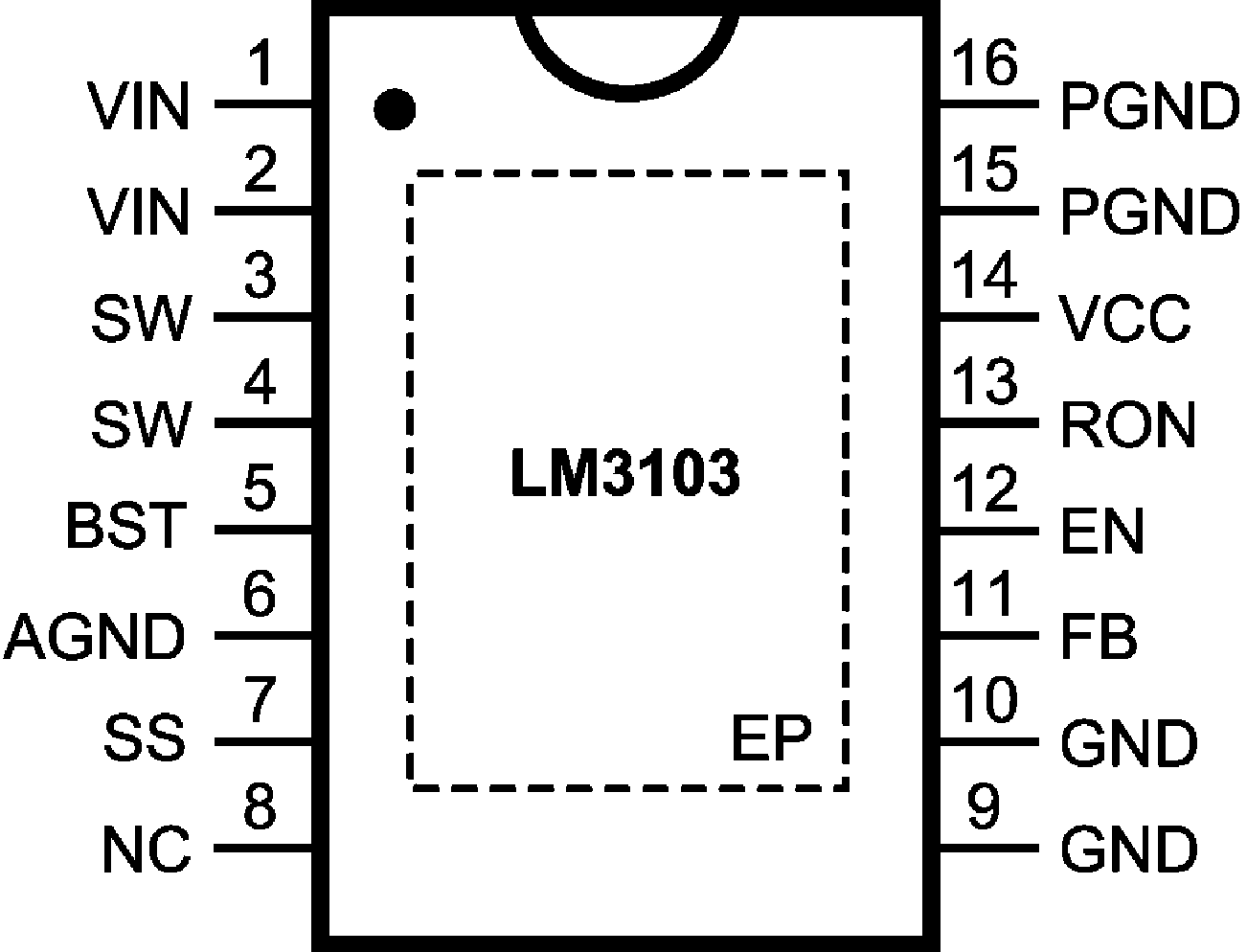
5 Pin Configuration and Functions
PWP Package
16-Pin HTSSOP
Top View

Pin Functions
| Pin | Name | Description | Application Information |
|---|---|---|---|
| 1, 2 | VIN | Input supply voltage | Supply pin to the device. Nominal input range is 4.5 V to 42 V. |
| 3, 4 | SW | Switch Node | Internally connected to the source of the main MOSFET and the drain of the synchronous MOSFET. Connect to the output inductor. |
| 5 | BST | Connection for bootstrap capacitor | Connect a 33 nF capacitor from the SW pin to this pin. This capacitor is charged through an internal diode during the main MOSFET off-time. |
| 6 | AGND | Analog Ground | Ground for all internal circuitry other than the PGND pin. |
| 7 | SS | Soft-start | A 70 µA internal current source charges an external capacitor of larger than 22 nF to provide the soft-start function. |
| 8 | NC | No Connection | This pin should be left unconnected. |
| 9, 10 | GND | Ground | Must be connected to the AGND pin for normal operation. The GND and AGND pins are not internally connected. |
| 11 | FB | Feedback | Internally connected to the regulation and over-voltage comparators. The regulation setting is 0.6 V at this pin. Connect to feedback resistors. |
| 12 | EN | Enable pin | Internal pull-up. Connect to a voltage higher than 1.6 V to enable the device. |
| 13 | RON | On-time Control | An external resistor from the VIN pin to this pin sets the main MOSFET on-time. |
| 14 | VCC | Startup regulator Output | Nominally regulated to 6 V. Connect a capacitor of larger than 1 µF between the VCC and AGND pins for stable operation. |
| 15, 16 | PGND | Power Ground | Synchronous MOSFET source connection. Tie to a ground plane. |
| DAP | EP | Exposed Pad | Thermal connection pad. Connect to the ground plane. |