SNVSAC2A March 2015 – June 2020 LM317A
PRODUCTION DATA.
- 1 Features
- 2 Applications
- 3 Description
- 4 Device Comparison Table
- 5 Pin Configuration and Functions
- 6 Specifications
- 7 Detailed Description
-
8 Application and Implementation
- 8.1 Application Information
- 8.2
Typical Applications
- 8.2.1 1.25-V to 25-V Adjustable Regulator
- 8.2.2 5-V Logic Regulator With Electronic Shutdown
- 8.2.3 Slow Turnon 15-V Regulator
- 8.2.4 Adjustable Regulator With Improved Ripple Rejection
- 8.2.5 High-Stability 10-V Regulator
- 8.2.6 High-Current Adjustable Regulator
- 8.2.7 Emitter-Follower Current Amplifier
- 8.2.8 1-A Current Regulator
- 8.2.9 Common-Emitter Amplifier
- 8.2.10 Low-Cost 3-A Switching Regulator
- 8.2.11 Current-Limited Voltage Regulator
- 8.2.12 Adjusting Multiple On-Card Regulators With Single Control
- 8.2.13 AC Voltage Regulator
- 8.2.14 12-V Battery Charger
- 8.2.15 Adjustable 4-A Regulator
- 8.2.16 Current-Limited 6-V Charger
- 8.2.17 Digitally-Selected Outputs
- 9 Power Supply Recommendations
- 10Layout
- 11Device and Documentation Support
- 12Mechanical, Packaging, and Orderable Information
封装选项
机械数据 (封装 | 引脚)
散热焊盘机械数据 (封装 | 引脚)
- DCY|4
订购信息
10.1.1.2.2 Heatsinking the TO-252 (NDP) Package
If the maximum allowable value for θJA is found to be ≥54°C/W (typical rated value) for the TO-252 package, no heatsink is needed because the package alone will dissipate enough heat to satisfy these requirements. If the calculated value for θJA falls below these limits, a heatsink is required.
As a design aid, Table 1 shows the value of the θJA of NDP the package for different heatsink area. The copper patterns that we used to measure these θJAs are shown in Figure 43. Figure 39 reflects the same test results as what are in Table 1.
Figure 40 shows the maximum allowable power dissipation versus ambient temperature for the TO-252 device. Figure 41 shows the maximum allowable power dissipation versus copper area (in2) for the TO-252 device. See the AN-1028 Maximum Power Enhancement Techniques for Power Packages application note for thermal enhancement techniques to be used with SOT-223 and TO-252 packages.
Table 1. θJA Different Heatsink Area
| Layout | Copper Area | Thermal Resistance | |
|---|---|---|---|
| Top Side (in2)(1) | Bottom Side (in2) | (θJA°C/W) TO-252 | |
| 1 | 0.0123 | 0 | 103 |
| 2 | 0.066 | 0 | 87 |
| 3 | 0.3 | 0 | 60 |
| 4 | 0.53 | 0 | 54 |
| 5 | 0.76 | 0 | 52 |
| 6 | 1 | 0 | 47 |
| 7 | 0.066 | 0.2 | 84 |
| 8 | 0.066 | 0.4 | 70 |
| 9 | 0.066 | 0.6 | 63 |
| 10 | 0.066 | 0.8 | 57 |
| 11 | 0.066 | 1 | 57 |
| 12 | 0.066 | 0.066 | 89 |
| 13 | 0.175 | 0.175 | 72 |
| 14 | 0.284 | 0.284 | 61 |
| 15 | 0.392 | 0.392 | 55 |
| 16 | 0.5 | 0.5 | 53 |
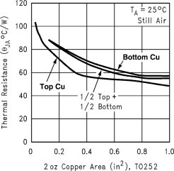 Figure 39. θJA vs 2-oz. Copper Area for TO-252
 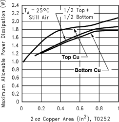 Figure 41. Maximum Allowable Power Dissipation vs 2-oz. Copper Area for TO-252
 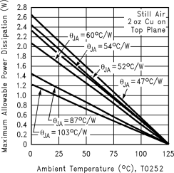 Figure 40. Maximum Allowable Power Dissipation vs Ambient Temperature for TO-252
 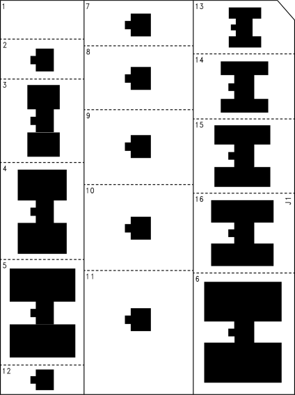 Figure 42. Top View of the Thermal Test Pattern in Actual Scale
 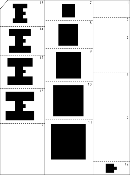 Figure 43. Bottom View of the Thermal Test Pattern in Actual Scale