SNVSAC2A March 2015 – June 2020 LM317A
PRODUCTION DATA.
- 1 Features
- 2 Applications
- 3 Description
- 4 Device Comparison Table
- 5 Pin Configuration and Functions
- 6 Specifications
- 7 Detailed Description
-
8 Application and Implementation
- 8.1 Application Information
- 8.2
Typical Applications
- 8.2.1 1.25-V to 25-V Adjustable Regulator
- 8.2.2 5-V Logic Regulator With Electronic Shutdown
- 8.2.3 Slow Turnon 15-V Regulator
- 8.2.4 Adjustable Regulator With Improved Ripple Rejection
- 8.2.5 High-Stability 10-V Regulator
- 8.2.6 High-Current Adjustable Regulator
- 8.2.7 Emitter-Follower Current Amplifier
- 8.2.8 1-A Current Regulator
- 8.2.9 Common-Emitter Amplifier
- 8.2.10 Low-Cost 3-A Switching Regulator
- 8.2.11 Current-Limited Voltage Regulator
- 8.2.12 Adjusting Multiple On-Card Regulators With Single Control
- 8.2.13 AC Voltage Regulator
- 8.2.14 12-V Battery Charger
- 8.2.15 Adjustable 4-A Regulator
- 8.2.16 Current-Limited 6-V Charger
- 8.2.17 Digitally-Selected Outputs
- 9 Power Supply Recommendations
- 10Layout
- 11Device and Documentation Support
- 12Mechanical, Packaging, and Orderable Information
封装选项
机械数据 (封装 | 引脚)
散热焊盘机械数据 (封装 | 引脚)
- DCY|4
订购信息
7.1 Overview
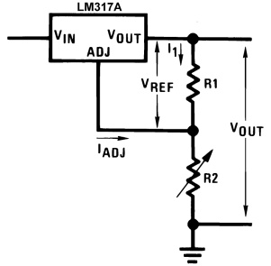
In operation, the LM317A develops a nominal 1.25-V reference voltage, VREF, between the output and adjustment terminal. The reference voltage is impressed across program resistor R1 and, because the voltage is constant, a constant current I1 then flows through the output set resistor R2 giving an output voltage calculated by Equation 1:

 Figure 15. Setting the VOUT Voltage
 Because the 100-μA current from the adjustment terminal represents an error term, the LM317A was designed to minimize IADJ and make it very constant with line and load changes. To do this, all quiescent operating current is returned to the output, establishing a minimum load current requirement. If there is insufficient load on the output, the output will rise.