SNOSC16D March 2000 – January 2015 LM124-N , LM224-N , LM2902-N , LM324-N
PRODUCTION DATA.
- 1 Features
- 2 Applications
- 3 Description
- 4 Revision History
- 5 Pin Configuration and Functions
- 6 Specifications
- 7 Detailed Description
- 8 Application and Implementation
- 9 Power Supply Recommendations
- 10Layout
- 11Device and Documentation Support
- 12Mechanical, Packaging, and Orderable Information
封装选项
机械数据 (封装 | 引脚)
散热焊盘机械数据 (封装 | 引脚)
订购信息
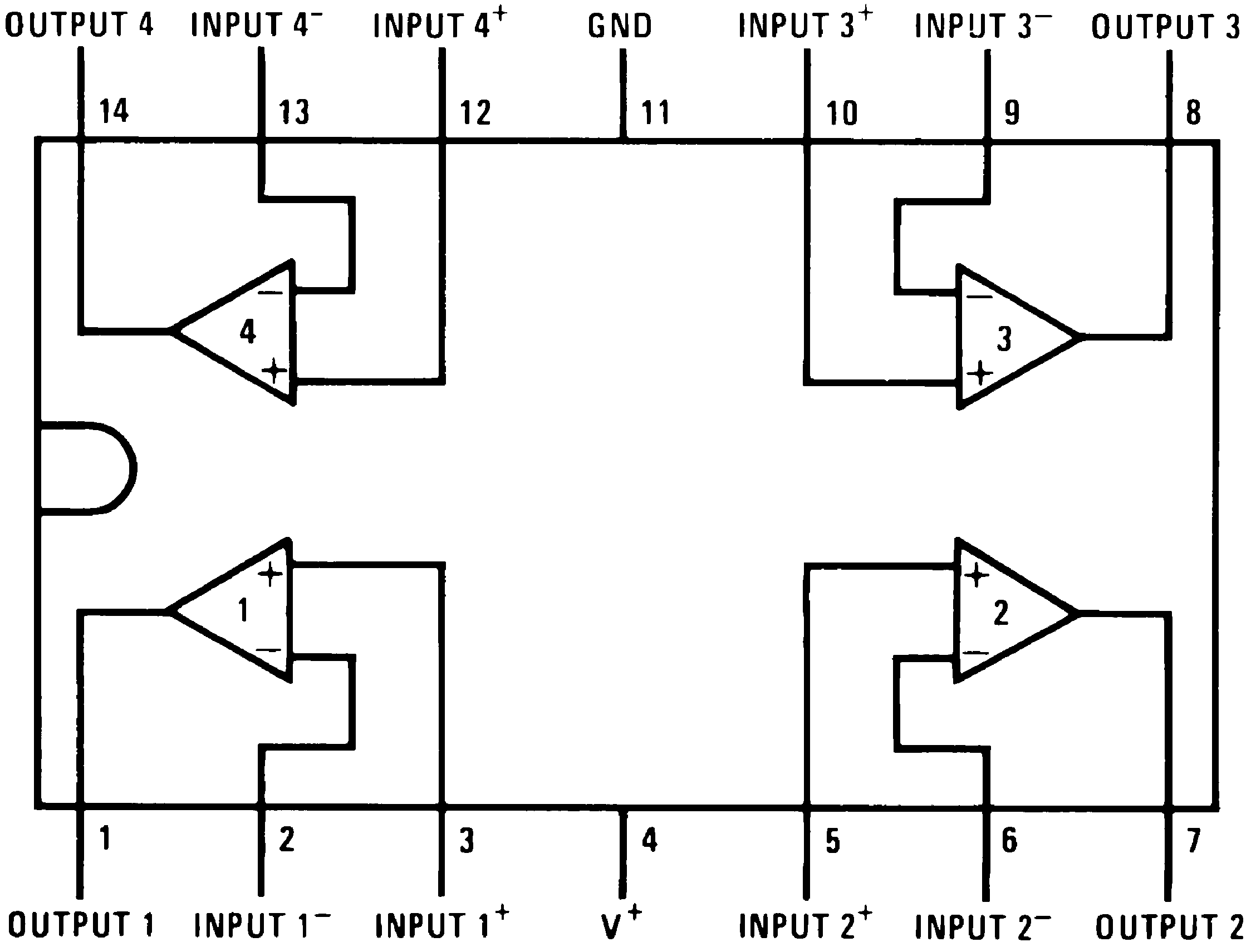
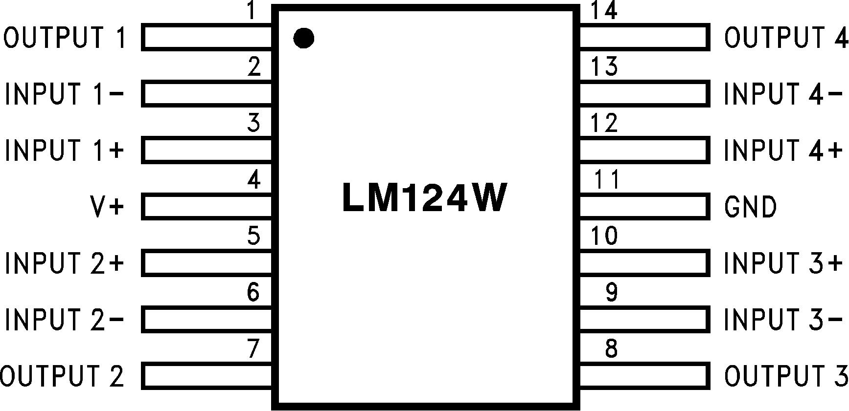
5 Pin Configuration and Functions
J Package
14-Pin CDIP
Top View

D Package
14-Pin SOIC
Top View

Pin Functions
| PIN | TYPE | DESCRIPTION | |
|---|---|---|---|
| NAME | NO. | ||
| OUTPUT1 | 1 | O | Output, Channel 1 |
| INPUT1- | 2 | I | Inverting Input, Channel 1 |
| INPUT1+ | 3 | I | Noninverting Input, Channel 1 |
| V+ | 4 | P | Positive Supply Voltage |
| INPUT2+ | 5 | I | Nonnverting Input, Channel 2 |
| INPUT2- | 6 | I | Inverting Input, Channel 2 |
| OUTPUT2 | 7 | O | Output, Channel 2 |
| OUTPUT3 | 8 | O | Output, Channel 3 |
| INPUT3- | 9 | I | Inverting Input, Channel 3 |
| INPUT3+ | 10 | I | Noninverting Input, Channel 3 |
| GND | 11 | P | Ground or Negative Supply Voltage |
| INPUT4+ | 12 | I | Noninverting Input, Channel 4 |
| INPUT4- | 13 | I | Inverting Input, Channel 4 |
| OUTPUT4 | 14 | O | Output, Channel 4 |