ZHCSGG3 June 2017 LM337-N-MIL
PRODUCTION DATA.
10 Layout
10.1 Layout Guidelines
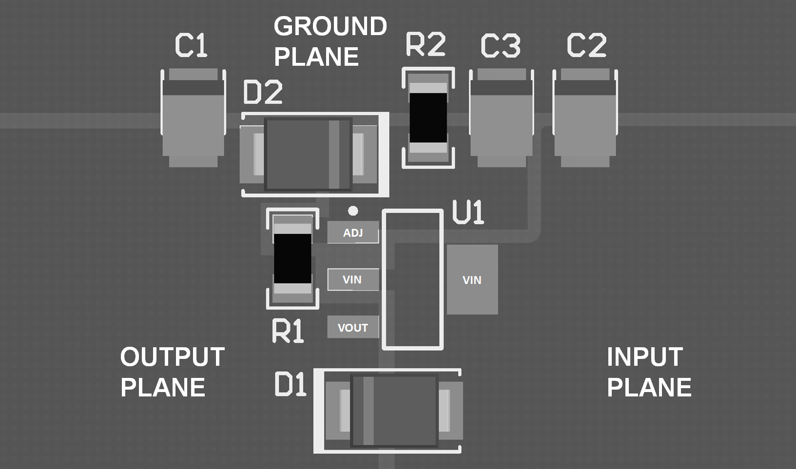
Some layout guidelines must be followed to ensure proper regulation of the output voltage with minimum noise. Traces carrying the load current must be wide to reduce the amount of parasitic trace inductance and the feedback loop from VOUT to ADJ must be kept as short as possible. To improve PSRR, a bypass capacitor can be placed at the ADJ pin and must be placed as close as possible to the IC. In cases when VIN shorts to ground, an external diode must be placed from VIN to VOUT to divert the surge current into the output capacitor and protect the IC. Similarly, in cases when a large bypass capacitor is placed at the ADJ pin and VOUT shorts to ground, an external diode must be placed from VOUT to ADJ to provide a path for the bypass capacitor to discharge. These diodes must be placed close to the corresponding IC pins to increase their effectiveness.
10.2 Layout Example
 Figure 16. Layout Example (SOT-223)
10.3 Thermal Considerations
10.3.1 Heatsinking SOT-223 Package Parts
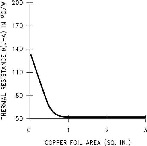
The SOT-223 DCY packages use a copper plane on the PCB and the PCB itself as a heatsink. To optimize the heat sinking ability of the plane and PCB, solder the tab of the package to the plane.
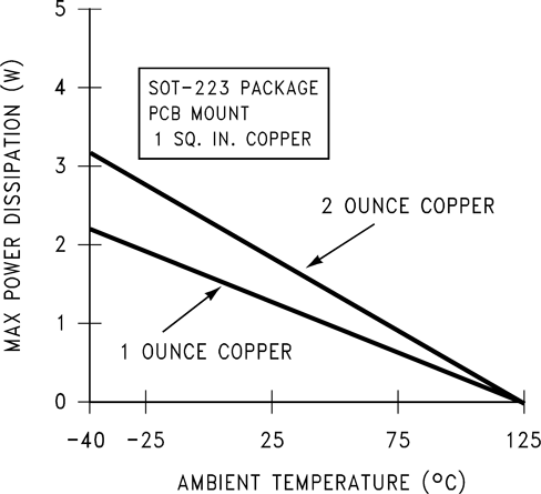
Figure 17 and Figure 18 show the information for the SOT-223 package. Figure 18 assumes a θ(J−A) of 75°C/W for 1 ounce copper and 51°C/W for 2 ounce copper and a maximum junction temperature of 125°C.
 Figure 17. θ(J−A) vs Copper (2 ounce) Area for the SOT-223 Package
 Figure 18. Maximum Power Dissipation vs TAMB for the SOT-223 Package
See AN-1028, SNVA036, for power enhancement techniques to be used with the SOT-223 package.