SNOSD54 June   2017 LM339-MIL

PRODUCTION DATA.  

  1. Features
  2. Applications
  3. Description
  4. Revision History
  5. Pin Configuration and Functions
  6. Specifications
    1. 6.1 Absolute Maximum Ratings
    2. 6.2 ESD Ratings
    3. 6.3 Recommended Operating Conditions
    4. 6.4 Thermal Information
    5. 6.5 Electrical Characteristics
    6. 6.6 Typical Characteristics
  7. Detailed Description
    1. 7.1 Overview
    2. 7.2 Functional Block Diagram
    3. 7.3 Feature Description
    4. 7.4 Device Functional Modes
  8. Application and Implementation
    1. 8.1 Application Information
    2. 8.2 Typical Application
      1. 8.2.1 Basic Comparator
        1. 8.2.1.1 Design Requirements
        2. 8.2.1.2 Application Curve
    3. 8.3 System Examples
      1. 8.3.1 Split-Supply Applications
  9. Power Supply Recommendations
  10. 10Layout
    1. 10.1 Layout Guidelines
    2. 10.2 Layout Example
  11. 11Device and Documentation Support
    1. 11.1 Documentation Support
      1. 11.1.1 Related Documentation
    2. 11.2 Receiving Notification of Documentation Updates
    3. 11.3 Community Resources
    4. 11.4 Trademarks
    5. 11.5 Electrostatic Discharge Caution
    6. 11.6 Glossary
  12. 12Mechanical, Packaging, and Orderable Information

封装选项

机械数据 (封装 | 引脚)
散热焊盘机械数据 (封装 | 引脚)
订购信息

Pin Configuration and Functions

J, D, and NFF Packages
14-Pin CDIP, SOIC, and PDIP
Top View
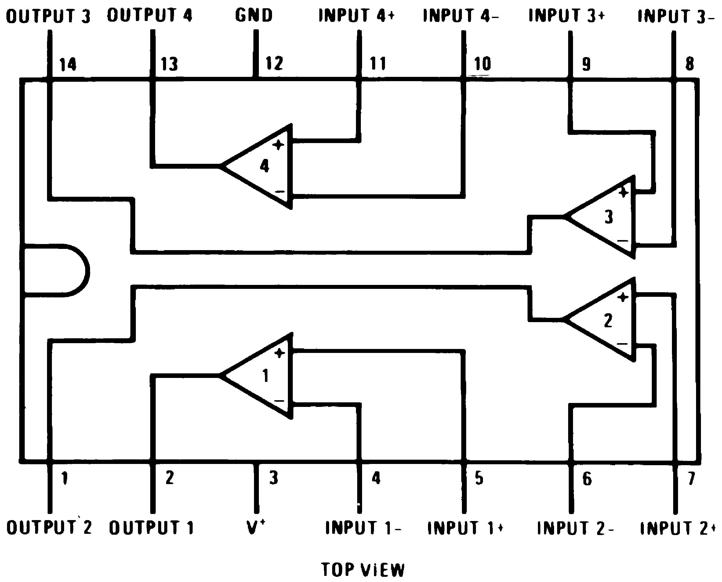
LM339-MIL lm339-mil-pinout-configuration.png

Pin Functions

PIN TYPE DESCRIPTION
NO. NAME
1 OUTPUT2 O Output, Channel 2
2 OUTPUT1 O Output, Channel 1
3 V+ P Positive Supply
4 INPUT1- I Inverting Input, Channel 1
5 INPUT1+ I Noninverting Input, Channel 1
6 INPUT2- I Inverting Input, Channel 2
7 INPUT2+ I Noninverting Input, Channel 2
8 INPUT3- I Inverting Input, Channel 3
9 INPUT3+ I Noninverting Input, Channel 3
10 INPUT4- I Inverting Input, Channel 4
11 INPUT4+ I Noninverting Input, Channel 4
12 GND P Ground
13 OUTPUT4 O Output, Channel 4
14 OUTPUT3 O Output, Channel 3