SNVS602L March 2009 – June 2016 LM3409 , LM3409-Q1 , LM3409HV , LM3409HV-Q1
PRODUCTION DATA.
- 1 Features
- 2 Applications
- 3 Description
- 4 Revision History
- 5 Device Comparison Table
- 6 Pin Configuration and Functions
- 7 Specifications
-
8 Detailed Description
- 8.1 Overview
- 8.2 Functional Block Diagram
- 8.3 Feature Description
- 8.4 Device Functional Modes
-
9 Application and Implementation
- 9.1
Application Information
- 9.1.1 Input Undervoltage Lockout (UVLO)
- 9.1.2 Operation Near Dropout
- 9.1.3 LED Ripple Current
- 9.1.4 Buck Converters without Output Capacitors
- 9.1.5 Buck Converters With Output Capacitors
- 9.1.6 Output Overvoltage Protection
- 9.1.7 Input Capacitors
- 9.1.8 P-Channel MOSFET (PFET)
- 9.1.9 Re-Circulating Diode
- 9.2
Typical Applications
- 9.2.1 EN PIN PWM Dimming Application for 10 LEDs
- 9.2.2 Analog Dimming Application for 4 LEDs
- 9.2.3 LM3409 Buck Converter Application
- 9.1
Application Information
- 10Power Supply Recommendations
- 11Layout
- 12Device and Documentation Support
- 13Mechanical, Packaging, and Orderable Information
9 Application and Implementation
NOTE
Information in the following applications sections is not part of the TI component specification, and TI does not warrant its accuracy or completeness. TI’s customers are responsible for determining suitability of components for their purposes. Customers should validate and test their design implementation to confirm system functionality.
9.1 Application Information
9.1.1 Input Undervoltage Lockout (UVLO)
Undervoltage lockout is set with a resistor divider from VIN to GND and is compared against a 1.24V threshold as shown in Figure 28. Once the input voltage is above the preset UVLO rising threshold (and assuming the part is enabled), the internal circuitry becomes active and a 22µA current source at the UVLO pin is turned on. This extra current provides hysteresis to create a lower UVLO falling threshold. The resistor divider is chosen to set both the UVLO rising and falling thresholds.
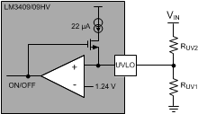 Figure 28. UVLO Circuit
The turn-on threshold (VTURN-ON) is defined as follows:

The hysteresis (VHYS) is defined as follows:

9.1.2 Operation Near Dropout
Because the power MOSFET is a PFET, the LM3409/09HV can be operated into dropout which occurs when the input voltage is approximately equal to output voltage. Once the input voltage drops below the nominal output voltage, the switch remains constantly on (D=1) causing the output voltage to decrease with the input voltage. In normal operation, the average LED current is regulated to the peak current threshold minus half of the ripple. As the converter goes into dropout, the LED current is exactly at the peak current threshold because it is no longer switching. This causes the LED current to increase by half of the set ripple current as it makes the transition into dropout. Therefore, the inductor current ripple should be kept as small as possible (while remaining above the previously established minimum) and output capacitance should be added to help maintain good line regulation when approaching dropout.
9.1.3 LED Ripple Current
Selection of the ripple current through the LED array is analogous to the selection of output ripple voltage in a standard voltage regulator. Where the output voltage ripple in a voltage regulator is commonly ±1% to ±5% of the DC output voltage, LED manufacturers generally recommend values for ΔiLED-PP ranging from ±5% to ±20% of ILED. For a nominal system operating point, a larger ΔiLED-PP specification can reduce the necessary inductor size and/or allow for smaller output capacitors (or no output capacitors at all) which helps to minimize the total solution size and cost. On the other hand, a smaller ΔiLED-PP specification would require more output inductance, a higher switching frequency, or additional output capacitance.
9.1.4 Buck Converters without Output Capacitors
Because current is being regulated, not voltage, a buck current regulator is free of load current transients, therefore output capacitance is not needed to supply the load and maintain output voltage. This is very helpful when high frequency PWM dimming the LED load. When no output capacitor is used, the same design equations that govern ΔiL-PP also apply to ΔiLED-PP.
9.1.5 Buck Converters With Output Capacitors
A capacitor placed in parallel with the LED load can be used to reduce ΔiLED-PP while keeping the same average current through both the inductor and the LED array. With an output capacitor, the inductance can be lowered, making the magnetics smaller and less expensive. Alternatively, the circuit can be run at lower frequency with the same inductor value, improving the efficiency and increasing the maximum allowable average output voltage. A parallel output capacitor is also useful in applications where the inductor or input voltage tolerance is poor. Adding a capacitor that reduces ΔiLED-PP to well below the target provides headroom for changes in inductance or VIN that might otherwise push the maximum ΔiLED-PP too high.
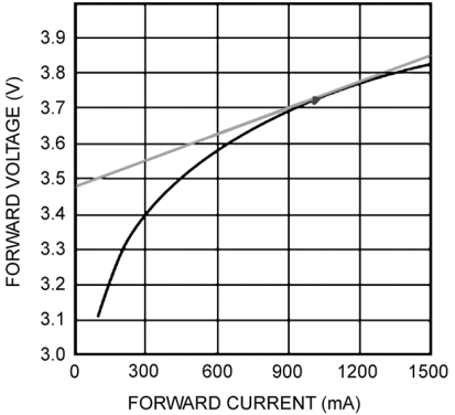 Figure 29. Calculating Dynamic Resistance rD
Output capacitance (CO) is determined knowing the desired ΔiLED-PP and the LED dynamic resistance (rD). rD can be calculated as the slope of the LED’s exponential DC characteristic at the nominal operating point as shown in Figure 29. Simply dividing the forward voltage by the forward current at the nominal operating point will give an incorrect value that is 5x to 10x too high. Total dynamic resistance for a string of n LEDs connected in series can be calculated as the rD of one device multiplied by n. The following equations can then be used to estimate ΔiLED-PP when using a parallel capacitor:


In general, ZC should be at least half of rD to effectively reduce the ripple. Ceramic capacitors are the best choice for the output capacitors due to their high ripple current rating, low ESR, low cost, and small size compared to other types. When selecting a ceramic capacitor, special attention must be paid to the operating conditions of the application. Ceramic capacitors can lose one-half or more of their capacitance at their rated DC voltage bias and also lose capacitance with extremes in temperature. Make sure to check any recommended de-ratings and also verify if there is any significant change in capacitance at the operating voltage and temperature.
9.1.6 Output Overvoltage Protection
Because the LM3409/09HV controls a buck current regulator, there is no inherent need to provide output overvoltage protection. If the LED load is opened, the output voltage will only rise as high as the input voltage plus any ringing due to the parasitic inductance and capacitance present at the output node. If a ceramic output capacitor is used in the application, it should have a minimum rating equal to the input voltage. Ringing seen at the output node should not damage most ceramic capacitors, due to their high ripple current rating.
9.1.7 Input Capacitors
Input capacitors are selected using requirements for minimum capacitance and RMS ripple current. The PFET current during tON is approximately ILED, therefore the input capacitors discharge the difference between ILED and the average input current (IIN) during tON. During tOFF, the input voltage source charges up the input capacitors with IIN. The minimum input capacitance (CIN-MIN) is selected using the maximum input voltage ripple (ΔvIN-MAX) which can be tolerated. ΔvIN-MAX is equal to the change in voltage across CIN during tON when it supplies the load current. A good starting point for selection of CIN is to use ΔvIN-MAX of 2% to 10% of VIN. CIN-MIN can be selected as follows:

An input capacitance at least 75% greater than the calculated CIN-MIN value is recommended. To determine the RMS input current rating (IIN-RMS) the following approximation can be used:

Because this approximation assumes there is no inductor ripple current, the value should be increased by 10-30% depending on the amount of ripple that is expected. Ceramic capacitors are the best choice for input capacitors for the same reasons mentioned in the Buck Converters With Output Capacitors section. Careful selection of the capacitor requires checking capacitance ratings at the nominal operating voltage and temperature.
9.1.8 P-Channel MOSFET (PFET)
The LM3409/09HV requires an external PFET (Q1) as the main power MOSFET for the switching regulator. Q1 should have a voltage rating at least 15% higher than the maximum input voltage to ensure safe operation during the ringing of the switch node. In practice all switching converters have some ringing at the switch node due to the diode parasitic capacitance and the lead inductance. The PFET should also have a current rating at least 10% higher than the average transistor current (IT):

The power rating is verified by calculating the power loss (PT) using the RMS transistor current (IT-RMS) and the PFET on-resistance (RDS-ON):


It is important to consider the gate charge of Q1. As the input voltage increases from a nominal voltage to its maximum input voltage, the COFT architecture will naturally increase the switching frequency. The dominant switching losses are determined by input voltage, switching frequency, and PFET total gate charge (Qg). The LM3409/09HV must provide and remove charge Qg from the input capacitance of Q1 to turn it on and off. This occurs more often at higher switching frequencies which requires more current from the internal regulator, thereby increasing internal power dissipation and eventually causing the LM3409/09HV to thermally cycle. For a given range of operating points the only effective way to reduce these switching losses is to minimize Qg.
A good rule of thumb is to limit Qg < 30nC (if the switching frequency remains below 300kHz for the entire operating range then a larger Qg can be considered). If a PFET with small RDS-ON and a high voltage rating is required, there may be no choice but to use a PFET with Qg > 30nC.
When using a PFET with Qg > 30nC, the bypass capacitor (CF) should not be connected to the VIN pin. This will ensure that peak current detection through RSNS is not affected by the charging of the PFET input capacitance during switching, which can cause false triggering of the peak detection comparator. Instead, CF should be connected from the VCC pin to the CSN pin which will cause a small DC offset in VCST and ultimately ILED, however it avoids the problematic false triggering.
In general, the PFET should be chosen to meet the Qg specification whenever possible, while minimizing RDS-ON. This will minimize power losses while ensuring the part functions correctly over the full operating range.
9.1.9 Re-Circulating Diode
A re-circulating diode (D1) is required to carry the inductor current during tOFF. The most efficient choice for D1 is a Schottky diode due to low forward voltage drop and near-zero reverse recovery time. Similar to Q1, D1 must have a voltage rating at least 15% higher than the maximum input voltage to ensure safe operation during the ringing of the switch node and a current rating at least 10% higher than the average diode current (ID):

The power rating is verified by calculating the power loss through the diode. This is accomplished by checking the typical diode forward voltage (VD) from the I-V curve on the product data sheet and calculating as follows:

In general, higher current diodes have a lower VD and come in better performing packages minimizing both power losses and temperature rise.
9.2 Typical Applications
9.2.1 EN PIN PWM Dimming Application for 10 LEDs
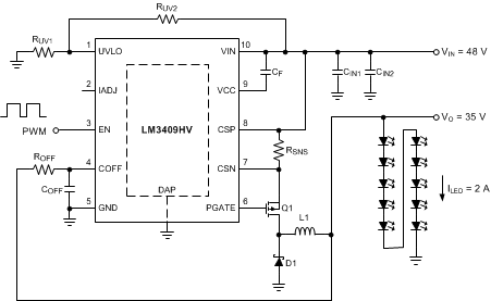 Figure 30. EN PIN PWM Dimming Application for 10 LEDs Schematic
9.2.1.1 Design Requirements
fSW = 525 kHz
VIN = 48 V; VIN-MAX = 75 V
VO = 35 V
ILED = 2 A
ΔiLED-PP = ΔiL-PP = 1 A
ΔvIN-PP = 1.44 V
VTURN-ON = 10 V; VHYS = 1.1 V
η = 0.95
9.2.1.2 Detailed Design Procedure
Table 1. Design 1 Bill of Materials
| QTY | PART ID | PART VALUE | MANUFACTURER | PART NUMBER |
|---|---|---|---|---|
| 1 | LM3409HV/LM3409QHV | Buck controller | TI | LM3409HVMY/LM3409QHVMY |
| 2 | CIN1, CIN2 | 2 µF X7R 10% 100 V | MURATA | GRM43ER72A225KA01L |
| 1 | CF | 1 µF X7R 10% 16 V | TDK | C1608X7R1C105K |
| 1 | COFF | 470 pF X7R 10% 50 V | TDK | C1608X7R1H471K |
| 1 | Q1 | PMOS 100 V 3.8 A | ZETEX | ZXMP10A18KTC |
| 1 | D1 | Schottky 100 V 3 A | VISHAY | SS3H10-E3/57T |
| 1 | L1 | 15 µH 20% 4.2 A | TDK | SLF12565T-150M4R2 |
| 1 | ROFF | 24.9 kΩ 1% | VISHAY | CRCW060324K9FKEA |
| 1 | RUV1 | 6.98 kΩ 1% | VISHAY | CRCW06036K98FKEA |
| 1 | RUV2 | 49.9 kΩ 1% | VISHAY | CRCW060349K9FKEA |
| 1 | RSNS | 0.1 Ω 1% 1W | VISHAY | WSL2512R1000FEA |
9.2.1.2.1 Nominal Switching Frequency
Assume COFF = 470 pF and η = 0.95. Solve for ROFF:

The closest 1% tolerance resistor is 24.9 kΩ; therefore, the actual tOFF and target fSW are:


The chosen components from step 1 are:

9.2.1.2.2 Inductor Ripple Current
Solve for L1:

The closest standard inductor value is 15 µH therefore the actual ΔiL-PP is:

The chosen component from step 2 is:

9.2.1.2.3 Average LED Current
Determine IL-MAX:

Assume VADJ = 1.24 V and solve for RSNS:

The closest 1% tolerance resistor is 0.1 Ω therefore the ILED is:

The chosen component from step 3 is:

9.2.1.2.4 Output Capacitance
No output capacitance is necessary.
9.2.1.2.5 Input Capacitance
Determine tON:

Solve for CIN-MIN:

Choose CIN:

Determine IIN-RMS:

The chosen components from step 5 are:

9.2.1.2.6 PFET
Determine minimum Q1 voltage rating and current rating:


A 100 V, 3.8 A PFET is chosen with RDS-ON = 19 0mΩ and Qg = 20 nC. Determine IT-RMS and PT:


The chosen component from step 6 is:

9.2.1.2.7 Diode
Determine minimum D1 voltage rating and current rating:


A 100-V, 3-A diode is chosen with VD = 750 mV. Determine PD:

The chosen component from step 7 is:

9.2.1.2.8 Input UVLO
Solve for RUV2:

The closest 1% tolerance resistor is 49.9 kΩ therefore VHYS is:

Solve for RUV1:

The closest 1% tolerance resistor is 6.98 kΩ therefore VTURN-ON is:

The chosen components from step 8 are:

9.2.1.2.9 IADJ Connection Method
The IADJ pin is left open forcing VADJ = 1.24 V.
9.2.1.2.10 PWM Dimming Method
PWM dimming signal pair is applied to the EN pin and GND at fDIM = 1 kHz.
9.2.1.3 Application Curve
Figure 31 shows the LED current versus EN pin PWM duty cycle for the application.
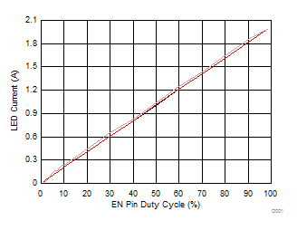
| Black = 200 Hz | Red = 1 kHz | Gray = 20 kHz |
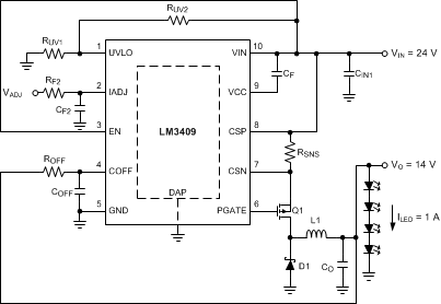
9.2.2 Analog Dimming Application for 4 LEDs
9.2.2.1 Design Requirements
fSW = 500 kHz
VIN = 24 V; VIN-MAX = 42 V
VO = 14 V
ILED = 1 A
ΔiL-PP = 450 mA; ΔiLED-PP = 50 mA
ΔvIN-PP = 1 V
VTURN-ON = 10 V; VHYS = 1.1 V
η = 0.90
9.2.2.2 Detailed Design Procedure
Table 2. Design 2 Bill of Materials
| QTY | PART ID | PART VALUE | MANUFACTURER | PART NUMBER |
|---|---|---|---|---|
| 1 | LM3409/LM3409Q | Buck controller | TI | LM3409MY/LM3409QMY |
| 2 | CIN1 | 4.7-µF X7R 10% 50 V | MURATA | GRM55ER71H475MA01L |
| 1 | CF | 1-µF X7R 10% 16 V | TDK | C1608X7R1C105K |
| 1 | CF2 | 0.1-µF X7R 10% 16 V | TDK | C1608X7R1C104K |
| 1 | COFF | 470-pF X7R 10% 50 V | TDK | C1608X7R1H471K |
| 1 | CO | 2.2-µF X7R 10% 50 V | MURATA | GRM43ER71H225MA01L |
| 1 | Q1 | PMOS 70 V 5.7 A | ZETEX | ZXMP7A17KTC |
| 1 | D1 | Schottky 60 V 5 A | COMCHIP | CDBC560-G |
| 1 | L1 | 22 µH 20% 4.2 A | TDK | SLF12575T-220M4R0 |
| 1 | RF2 | 1 kΩ 1% | VISHAY | CRCW06031K00FKEA |
| 1 | ROFF | 15.4 kΩ 1% | VISHAY | CRCW060315K4FKEA |
| 1 | RUV1 | 6.98 kΩ 1% | VISHAY | CRCW06036K98FKEA |
| 1 | RUV2 | 49.9 kΩ 1% | VISHAY | CRCW060349K9FKEA |
| 1 | RSNS | 0.2 Ω 1% 1W | VISHAY | WSL2512R2000FEA |
9.2.2.2.1 Nominal Switching Frequency
Assume COFF = 470 pF and η = 0.90. Solve for ROFF:
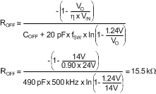
The closest 1% tolerance resistor is 15.4 kΩ; therefore, the actual tOFF and target fSW are:


The chosen components from step 1 are:

9.2.2.2.2 Inductor Ripple Current
Solve for L1:

The closest standard inductor value is 22 µH; therefore, the actual ΔiL-PP is:

The chosen component from step 2 is:

9.2.2.2.3 Average LED Current
Determine IL-MAX:

Assume VADJ = 1.24 V and solve for RSNS:

The closest 1% tolerance resistor is 0.2 Ω therefore ILED is:

The chosen component from step 3 is:

9.2.2.2.4 Output Capacitance
Assume rD = 2 Ω and determine ZC:

Solve for CO-MIN and :

Choose CO:

The chosen component from step 5 is:

9.2.2.2.5 Input Capacitance
Determine tON:

Solve for CIN-MIN:

Choose CIN:

Determine IIN-RMS:

The chosen component from step 5 is:

9.2.2.2.6 PFET
Determine minimum Q1 voltage rating and current rating:


A 70V, 5.7 A PFET is chosen with RDS-ON = 190 mΩ and Qg = 20 nC. Determine IT-RMS and PT:
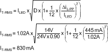

The chosen component from step 6 is:

9.2.2.2.7 Diode
Determine minimum D1 voltage rating and current rating:


A 60 V, 5 A diode is chosen with VD = 750 mV. Determine PD:

The chosen component from step 7 is:

9.2.2.2.8 Input UVLO
Solve for RUV2:

The closest 1% tolerance resistor is 49.9 kΩ therefore VHYS is:

Solve for RUV1:

The closest 1% tolerance resistor is 6.98 kΩ therefore VTURN-ON is:

The chosen components from step 8 are:

9.2.2.2.9 IADJ Connection Method
The IADJ pin is connected to an external voltage source and varied from 0 – 1.24 V to dim. An RC filter (RF2 = 1 kΩ and CF2 = 0.1 µF) is used as recommended.
9.2.2.2.10 PWM Dimming Method
No PWM dimming is necessary.
9.2.2.3 Application Curve
Figure 32 shows the LED current versus IADJ voltage for the application.
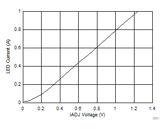 Figure 32. Analog Dimming Profile
9.2.3 LM3409 Buck Converter Application
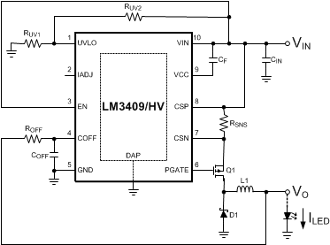 Figure 33. LM3409 Buck Converter Simplified Schematic
9.2.3.1 Design Requirements
Nominal input voltage: VIN
Maximum input voltage: VIN-MAX
Nominal output voltage (number of LEDs x forward voltage): VO
LED string dynamic resistance: rD
Switching frequency (at nominal VIN, VO): fSW
Average LED current: ILED
Inductor current ripple: ΔiL-PP
LED current ripple: ΔiLED-PP
Input voltage ripple: ΔvIN-PP
UVLO characteristics: VTURN-ON and VHYS
Expected efficiency: η
9.2.3.2 Detailed Design Procedure
9.2.3.2.1 Nominal Switching Frequency
Calculate switching frequency (fSW) at the nominal operating point (VIN and VO). Assume a COFF value (from 470 pF to 1 nF) and a system efficiency (η). Solve for ROFF:

9.2.3.2.2 Inductor Ripple Current
Set the inductor ripple current (ΔiL-PP) by solving for the appropriate inductor (L1):

9.2.3.2.3 Average LED Current
Set the average LED current (ILED) by first solving for the peak inductor current (IL-MAX):

Peak inductor current is detected across the sense resistor (RSNS). In most cases, assume the maximum value (VADJ = 1.24 V) at the IADJ pin and solve for RSNS:

If the calculated RSNS is far from a standard value, the beginning of the process can be iterated to choose a new ROFF, L1, and RSNS value that is a closer fit. The easiest way to approach the iterative process is to change the nominal fSW target knowing that the switching frequency varies with operating conditions anyways.
Another method for finding a standard RSNS value is to change the VADJ value. However, this would require an external voltage source or a resistor from the IADJ pin to GND as explained in the Adjustable Peak Current Control section of this data sheet.
9.2.3.2.4 Output Capacitance
A minimum output capacitance (CO-MIN) may be necessary to reduce ΔiLED-PP below ΔiL-PP. With the specified ΔiLED-PP and the known dynamic resistance (rD) of the LED string, solve for the required impedance (ZC) for CO-MIN:

Solve for CO-MIN:

9.2.3.2.5 Input Capacitance
Set the input voltage ripple (ΔvIN-PP) by solving for the required minimum capacitance (CIN-MIN):

The necessary RMS input current rating (IIN-RMS) is:

9.2.3.2.6 PFET
The PFET voltage rating should be at least 15% higher than the maximum input voltage (VIN-MAX) and current rating should be at least 10% higher than the average PFET current (IT):

Given a PFET with on-resistance (RDS-ON), solve for the RMS transistor current (IT-RMS) and power dissipation (PT):


9.2.3.2.7 Diode
The Schottky diode needs a voltage rating similar to the PFET. Higher current diodes with a lower forward voltage are suggested. Given a diode with forward voltage (VD), solve for the average diode current (ID) and power dissipation (PD):


9.2.3.2.8 Input UVLO
Input UVLO is set with the turnon threshold voltage (VTURN-ON) and the desired hysteresis (VHYS). To set VHYS, solve for RUV2:

To set VTURN-ON, solve for RUV1:

9.2.3.2.9 IADJ Connection Method
The IADJ pin controls the high-side current sense threshold in three ways outlined in the Adjustable Peak Current Control section.
Method 1: Leave IADJ pin open and ILED is calculated as in the Average LED Current section of the Design Guide.
Method 2: Apply an external voltage (VADJ) to the IADJ pin from 0 to 1.24 V to analog dim or to reduce ILED as follows:

Keep in mind that analog dimming will eventually push the converter in to DCM and the inductor current ripple will no longer be constant causing a divergence from linear dimming at low levels.
A 0.1 µF capacitor connected from the IADJ pin to GND is recommended when using this method. It may also be necessary to have a 1kΩ series resistor with the capacitor to create an RC filter. The filter will help remove high frequency noise created by other connected circuitry.
Method 3: Connect an external resistor or potentiometer to GND (REXT) and the internal 5 µA current source will set the voltage. Again, a 0.1 µF capacitor connected from the IADJ pin to GND is recommended. To set ILED, solve for REXT:

9.2.3.2.10 PWM Dimming Method
There are two methods to PWM dim using the LM3409/09HV:
Method 1:Apply an external PWM signal to the EN terminal.
Method 2: Perform external parallel FET shunt dimming as detailed in the External Parallel FET PWM Dimming section.