SNVS678F June 2010 – November 2015 LM3414 , LM3414HV
PRODUCTION DATA.
- 1 Features
- 2 Applications
- 3 Description
- 4 Revision History
- 5 Pin Configuration and Functions
- 6 Specifications
- 7 Detailed Description
- 8 Application and Implementation
- 9 Power Supply Recommendations
- 10Layout
- 11Device and Documentation Support
- 12Mechanical, Packaging, and Orderable Information
封装选项
机械数据 (封装 | 引脚)
散热焊盘机械数据 (封装 | 引脚)
- DDA|8
订购信息
8 Application and Implementation
NOTE
Information in the following applications sections is not part of the TI component specification, and TI does not warrant its accuracy or completeness. TI’s customers are responsible for determining suitability of components for their purposes. Customers should validate and test their design implementation to confirm system functionality.
8.1 Application Information
8.1.1 Setting the Switching Frequency
Both the LM3414 and LM3414HV are PWM LED drivers that contain a clock generator to generate constant switching frequency for the device. The switching frequency is determined by the resistance of an external resistor RFS in the range of 250 kHz to 1 MHz. Lower resistance of RFS results in higher switching frequency. The switching frequency of the LM3414/HV is governed using Equation 5.

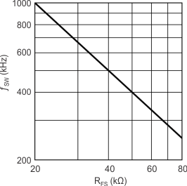 Figure 20. Switching Frequency vs RFS
Table 1. Examples for fSW Settings
| fSW (kHz) | RFS (kΩ) |
|---|---|
| 250 | 80 |
| 500 | 40 |
| 1000 | 20 |
To ensure accurate current regulation, the LM3414/HV should be operated in continuous conduction mode (CCM) and the ON time should not be shorter than 400 ns under all operation condition.
8.1.2 Setting LED Current
The LM3414/HV requires no external current sensing resistor for LED current regulation. The average output current of the LM3414/HV is adjustable by varying the resistance of the resistor, RIADJ that connects across the IADJ and GND pins. The IADJ pin is internally biased to 1.255 V. The LED current is then governed by Equation 6.

where
- 350 mA < ILED < 1A
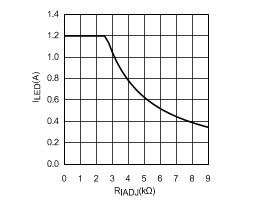 Figure 21. LED Current vs RIADJ
Table 2. Examples for IOUT Settings
| IOUT (mA) | RIADJ (kΩ) |
|---|---|
| 350 | 8.93 |
| 500 | 6.25 |
| 700 | 4.46 |
| 1000 | 3.13 |
The LED current can be set to any level in the range from 350 mA to 1A. To provide accurate LED current, RIADJ should be a resistor with no more than 0.5% tolerance. If the IADJ pin is accidentally shorted to GND (RIADJ = 0), the output current is limited to avoid damaging the circuit. When the overcurrent protection is activated, current regulation cannot be maintained until the overcurrent condition is cleared.
8.1.3 Inductor Selection
To ensure proper output current regulation, the LM3414/HV must operate in Continuous Conduction Mode (CCM). With the incorporation of PLM, the peak-to-peak inductor current ripple can be set as high as ±60% of the defined average output current. The minimum inductance of the inductor is decided by the defined average LED current and allowable inductor current ripple. The minimum inductance can be found by the equations shown in Equation 7 through Equation 8.
Because:

Thus:

The LM3414/HV can maintain LED current regulation without output filter capacitor. This is because the inductor of the floating buck structure provides continuous current to the LED throughout the entire switching cycle. When LEDs are driven without filter capacitor, the LED peak current must not set exceeding the rated current of the LED. The peak LED current is governed by Equation 9.

8.2 Typical Applications
8.2.1 LM3414/HV Design Example
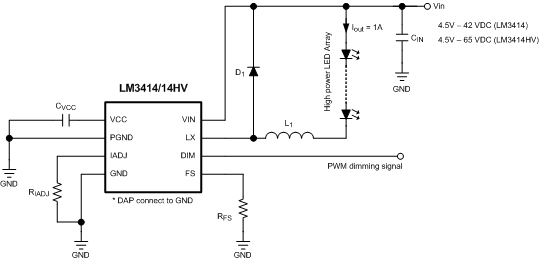 Figure 22. LM3414/HV Design Example Schematic
8.2.1.1 Design Requirements
- Input Voltage: VIN
- LED String Voltage: VLED
- LED Current: ILED
- Switching Frequency: fSW
- Maximum LED Current Ripple: ΔiL-PP
- Maximum Input Voltage Ripple: ΔVIN
8.2.1.2 Detailed Design Procedure
8.2.1.2.1 Calculate Operating Parameters
To calculate component values the operating duty cycle (D) must be calculated using Equation 10.

8.2.1.2.2 Calculate RIADJ
To get the desired LED current calculate the value for RIADJ using Equation 11.

8.2.1.2.3 Calculate RFS
Calculate the value of RFS for the desired switching frequency using Equation 12.

8.2.1.2.4 Calculate LMIN
Calculate the minimum inductor value required for the desired LED current ripple using Equation 13.

8.2.1.2.5 Calculate CIN-MIN
Calculate the minimum input capacitor value for the desired input voltage ripple using Equation 14.

8.2.2 LM3414/HV Design Example (IOUT = 1 A)
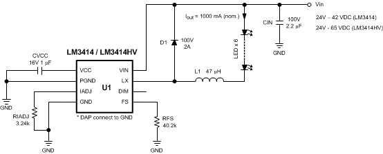 Figure 23. LM3414/HV Design Example (IOUT = 1 A) Schematic
8.2.2.1 Design Requirements
- Input Voltage: VIN = 48 V ±10%
- LED String Voltage: VLED = 35 V
- LED Current: ILED = 1 A
- Switching Frequency: fSW = 500 kHz
- Maximum LED Current Ripple: ΔiL-PP ≤ 500 mA
- Maximum Input Voltage Ripple: ΔVIN ≤ 200 mV
8.2.2.2 Detailed Design Procedure
8.2.2.2.1 Calculate Operating Parameters
To calculate component values the operating duty cycle (D) for this application can be calculated be calculated using Equation 15.

8.2.2.2.2 Calculate RIADJ
For 1A LED current calculate the value for RIADJ using Equation 16.

Choose a standard value of RIADJ = 3.24kΩ.
8.2.2.2.3 Calculate RFS
Calculate the value of RFS for 500-kHz switching frequency using Equation 17.

Choose a standard value of RFS = 40.2kΩ.
8.2.2.2.4 Calculate LMIN
Calculate the minimum inductor value required for 500 mA or less peak-to-peak LED current ripple using Equation 18.

Choose a higher standard value of L = 47µH.
8.2.2.2.5 Calculate CIN-MIN
Calculate the minimum input capacitor value for 200 mV or less input voltage ripple using Equation 19.

Choose a higher standard value of CIN = 2.2µF.
Table 3. Bill of Materials
| DESIGNATION | DESCRIPTION | PACKAGE | MANUFACTURE PART NO. | VENDOR |
|---|---|---|---|---|
| U1 | LED Driver IC LM3414 / LM3414HV |
SOIC-8 | LM3414 / LM3414HV | TI |
| L1 | Inductor 47 µH | 8 × 8 × 4.9 (mm) | MMD-08EZ-470M-SI | Mag.Layers |
| D1 | Schottky Diode 100 V, 2 A | SMP | SS2PH10-M3 | Vishay |
| CIN | Cap MLCC 100V 2.2 µF X7R | 1210 | GRM32ER72A225KA35L | Murata |
| CVCC | Cap MLCC 16V 1 µF X5R | 603 | GRM39X5R105K16D52K | Murata |
| RIADJ | Chip Resistor 3.24 kΩ 1% | 603 | CRCW06033241F | Vishay |
| RFS | Chip Resistor 40.2 kΩ 1% | 603 | CRCW06034022F | Vishay |
8.2.2.3 Application Curve
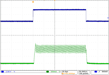 Figure 24. PWM Dimming Top = DIM. Bottom = LED Current.