SNVSB95 July 2019 LM3421-Q1 , LM3423-Q1
PRODUCTION DATA.
- 1 Features
- 2 Applications
- 3 Description
- 4 Revision History
- 5 Device Comparison
- 6 Pin Configuration and Functions
- 7 Specifications
-
8 Detailed Description
- 8.1 Overview
- 8.2 Functional Block Diagram
- 8.3
Feature Description
- 8.3.1 Current Regulators
- 8.3.2 Predictive Off-Time (PRO) Control
- 8.3.3 Average LED Current
- 8.3.4 Analog Dimming
- 8.3.5 Current Sense and Current Limit
- 8.3.6 Overcurrent Protection
- 8.3.7 Zero Current Shutdown
- 8.3.8 Control Loop Compensation
- 8.3.9 Start-Up Regulator
- 8.3.10 Overvoltage Lockout (OVLO)
- 8.3.11 Input Undervoltage Lockout (UVLO)
- 8.3.12 PWM Dimming
- 8.3.13 LM3423-Q1 Only: DPOL, FLT, TIMR, and LRDY
-
9 Application and Implementation
- 9.1 Application Information
- 9.2
Typical Applications
- 9.2.1
Basic Topology Schematics
- 9.2.1.1 Design Requirements
- 9.2.1.2
Detailed Design Procedure
- 9.2.1.2.1 Operating Point
- 9.2.1.2.2 Switching Frequency
- 9.2.1.2.3 Average LED Current
- 9.2.1.2.4 Inductor Ripple Current
- 9.2.1.2.5 LED Ripple Current
- 9.2.1.2.6 Peak Current Limit
- 9.2.1.2.7 Loop Compensation
- 9.2.1.2.8 Input Capacitance
- 9.2.1.2.9 N-channel FET
- 9.2.1.2.10 Diode
- 9.2.1.2.11 Output OVLO
- 9.2.1.2.12 Input UVLO
- 9.2.1.2.13 PWM Dimming Method
- 9.2.1.2.14 Analog Dimming Method
- 9.2.2
LM3421 Buck-Boost Application
- 9.2.2.1 Design Requirements
- 9.2.2.2
Detailed Design Procedure
- 9.2.2.2.1 Operating Point
- 9.2.2.2.2 Switching Frequency
- 9.2.2.2.3 Average LED Current
- 9.2.2.2.4 Inductor Ripple Current
- 9.2.2.2.5 Output Capacitance
- 9.2.2.2.6 Peak Current Limit
- 9.2.2.2.7 Loop Compensation
- 9.2.2.2.8 Input Capacitance
- 9.2.2.2.9 N-channel FET
- 9.2.2.2.10 Diode
- 9.2.2.2.11 Input UVLO
- 9.2.2.2.12 Output OVLO
- 9.2.2.3 Application Curve
- 9.2.3 LM3421-Q1 BOOST Application
- 9.2.4 LM3421-Q1 Buck-Boost Application
- 9.2.5 LM3423-Q1 Boost Application
- 9.2.6 LM3421 Buck-Boost Application
- 9.2.7 LM3423 Buck Application
- 9.2.8 LM3423 Buck-Boost Application
- 9.2.9 LM3421 SEPIC Application
- 9.2.1
Basic Topology Schematics
- 10Power Supply Recommendations
- 11Layout
- 12Device and Documentation Support
- 13Mechanical, Packaging, and Orderable Information
8.3.5 Current Sense and Current Limit
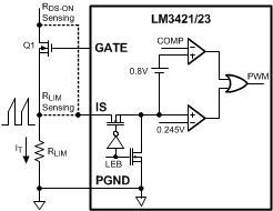
The LM3421-Q1 and LM3423-Q1 achieve peak current mode control using a comparator that monitors the main MOSFET (Q1) transistor current, comparing it with the COMP pin voltage as shown in Figure 15. The controller incorporates a cycle-by-cycle overcurrent protection function. Aredundant internal current sense comparator provides the current limit functionality . If the voltage at the current sense comparator input (IS pin) exceeds 245 mV (typical), the on cycle is immediately terminated. The IS input pin has an internal N-channel MOSFET which pulls it down at the conclusion of every cycle. The discharge device remains on for an additional 210 ns (typical) after the beginning of a new cycle to blank the leading edge spike on the current sense signal. The leading edge blanking (LEB) determines the minimum achievable on-time (tON-MIN).
 Figure 15. Current Sense / Current Limit Circuitry
 There are two possible methods to sense the transistor current. The RDS-ON of the main power MOSFET can be used as the current sense resistance because the IS pin was designed to withstand the high voltages present on the drain when the MOSFET is in the off state. Alternatively, a sense resistor located in the source of the MOSFET may be used for current sensing; however, TI suggests a low inductance (ESL) type. The cycle-by-cycle current limit (ILIM) can be calculated using either method as the limiting resistance (RLIM):
