SNVSB96 July 2019 LM3424-Q1
PRODUCTION DATA.
- 1 Features
- 2 Applications
- 3 Description
- 4 Revision History
- 5 Pin Configuration and Functions
- 6 Specifications
-
7 Detailed Description
- 7.1 Overview
- 7.2 Functional Block Diagram
- 7.3
Feature Description
- 7.3.1 Current Regulators
- 7.3.2 Peak Current Mode Control
- 7.3.3 Average LED Current
- 7.3.4 Thermal Foldback and Analog Dimming
- 7.3.5 Current Sense and Current Limit
- 7.3.6 Slope Compensation
- 7.3.7 Control Loop Compensation
- 7.3.8 Start-Up Regulator and Soft-Start
- 7.3.9 Overvoltage Lockout (OVLO)
- 7.3.10 Input Undervoltage Lockout (UVLO)
- 7.3.11 PWM Dimming
- 7.3.12 Thermal Shutdown
- 7.4 Device Functional Modes
-
8 Application and Implementation
- 8.1 Application Information
- 8.2
Typical Applications
- 8.2.1
Basic Topology Schematics
- 8.2.1.1 Design Requirements
- 8.2.1.2
Detailed Design Procedure
- 8.2.1.2.1 Operating Point
- 8.2.1.2.2 Switching Frequency
- 8.2.1.2.3 Average LED Current
- 8.2.1.2.4 Thermal Foldback
- 8.2.1.2.5 Inductor Ripple Current
- 8.2.1.2.6 LED Ripple Current
- 8.2.1.2.7 Peak Current Limit
- 8.2.1.2.8 Slope Compensation
- 8.2.1.2.9 Loop Compensation
- 8.2.1.2.10 Input Capacitance
- 8.2.1.2.11 NFET
- 8.2.1.2.12 Diode
- 8.2.1.2.13 Output OVLO
- 8.2.1.2.14 Input UVLO
- 8.2.1.2.15 Soft-Start
- 8.2.1.2.16 PWM Dimming Method
- 8.2.1.2.17 Analog Dimming Method
- 8.2.2
Buck-Boost Application
- 8.2.2.1 Design Requirements
- 8.2.2.2
Detailed Design Procedure
- 8.2.2.2.1 Operating Point
- 8.2.2.2.2 Switching Frequency
- 8.2.2.2.3 Average LED Current
- 8.2.2.2.4 Thermal Foldback
- 8.2.2.2.5 Inductor Ripple Current
- 8.2.2.2.6 Output Capacitance
- 8.2.2.2.7 Peak Current Limit
- 8.2.2.2.8 Slope Compensation
- 8.2.2.2.9 Loop Compensation
- 8.2.2.2.10 Input Capacitance
- 8.2.2.2.11 NFET
- 8.2.2.2.12 Diode
- 8.2.2.2.13 Input UVLO
- 8.2.2.2.14 Output OVLO
- 8.2.2.2.15 Soft-Start
- 8.2.2.3 Application Curve
- 8.2.3 Boost Application
- 8.2.4 Buck-Boost Application
- 8.2.5 Boost Application
- 8.2.6 Buck-Boost Application
- 8.2.7 Buck Application
- 8.2.8 Buck-Boost Application
- 8.2.9 SEPIC Application
- 8.2.1
Basic Topology Schematics
- 9 Power Supply Recommendations
- 10Layout
- 11Device and Documentation Support
- 12Mechanical, Packaging, and Orderable Information
7.3.3 Average LED Current
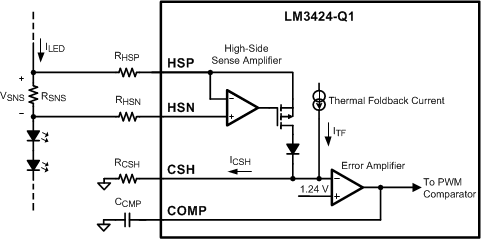
To first understand how the LM3424-Q1 regulates LED current, the thermal foldback functionality will be ignored. Figure 18 shows the physical implementation of the LED current sense circuitry assuming the thermal foldback circuitry is a simple current source which, for now, will be set to zero (ITF = 0A). The LM3424-Q1 uses an external current sense resistor (RSNS) placed in series with the LED load to convert the LED current (ILED) into a voltage (VSNS). The HSP and HSN pins are the inputs to the high-side sense amplifier which are forced to be equal potential (VHSP=VHSN) through negative feedback. Because of this, the VSNS voltage is forced across RHSP which generates a current that is summed with the thermal foldback current (ITF) to generate the signal current (ICSH) which flows out of the CSH pin and through the RCSH resistor. The error amplifier will regulate the CSH pin to 1.24V and assuming ITF = 0A, ICSH can be calculated:

This means VSNS will be regulated as follows:

ILED can then be calculated:

The selection of the three resistors (RSNS, RCSH, and RHSP) is not arbitrary. For matching and noise performance, the suggested signal current ICSH is approximately 100 µA. This current does not flow in the LEDs and will not affect either the off-state LED current or the regulated LED current. ICSH can be above or below this value, but the high-side amplifier offset characteristics may be affected slightly. In addition, to minimize the effect of the high-side amplifier voltage offset on LED current accuracy, the minimum VSNS is suggested to be 50 mV. Finally, a resistor (RHSN = RHSP) should be placed in series with the HSN pin to cancel out the effects of the input bias current (~10 µA) of both inputs of the high-side sense amplifier.
Note that he CSH pin can also be used as a low-side current sense input regulated to 1.24V. The high-side sense amplifier is disabled if HSP and HSN are tied to GND.
 Figure 18. LED Current Sense Circuitry