SNVSB96 July 2019 LM3424-Q1
PRODUCTION DATA.
- 1 Features
- 2 Applications
- 3 Description
- 4 Revision History
- 5 Pin Configuration and Functions
- 6 Specifications
-
7 Detailed Description
- 7.1 Overview
- 7.2 Functional Block Diagram
- 7.3
Feature Description
- 7.3.1 Current Regulators
- 7.3.2 Peak Current Mode Control
- 7.3.3 Average LED Current
- 7.3.4 Thermal Foldback and Analog Dimming
- 7.3.5 Current Sense and Current Limit
- 7.3.6 Slope Compensation
- 7.3.7 Control Loop Compensation
- 7.3.8 Start-Up Regulator and Soft-Start
- 7.3.9 Overvoltage Lockout (OVLO)
- 7.3.10 Input Undervoltage Lockout (UVLO)
- 7.3.11 PWM Dimming
- 7.3.12 Thermal Shutdown
- 7.4 Device Functional Modes
-
8 Application and Implementation
- 8.1 Application Information
- 8.2
Typical Applications
- 8.2.1
Basic Topology Schematics
- 8.2.1.1 Design Requirements
- 8.2.1.2
Detailed Design Procedure
- 8.2.1.2.1 Operating Point
- 8.2.1.2.2 Switching Frequency
- 8.2.1.2.3 Average LED Current
- 8.2.1.2.4 Thermal Foldback
- 8.2.1.2.5 Inductor Ripple Current
- 8.2.1.2.6 LED Ripple Current
- 8.2.1.2.7 Peak Current Limit
- 8.2.1.2.8 Slope Compensation
- 8.2.1.2.9 Loop Compensation
- 8.2.1.2.10 Input Capacitance
- 8.2.1.2.11 NFET
- 8.2.1.2.12 Diode
- 8.2.1.2.13 Output OVLO
- 8.2.1.2.14 Input UVLO
- 8.2.1.2.15 Soft-Start
- 8.2.1.2.16 PWM Dimming Method
- 8.2.1.2.17 Analog Dimming Method
- 8.2.2
Buck-Boost Application
- 8.2.2.1 Design Requirements
- 8.2.2.2
Detailed Design Procedure
- 8.2.2.2.1 Operating Point
- 8.2.2.2.2 Switching Frequency
- 8.2.2.2.3 Average LED Current
- 8.2.2.2.4 Thermal Foldback
- 8.2.2.2.5 Inductor Ripple Current
- 8.2.2.2.6 Output Capacitance
- 8.2.2.2.7 Peak Current Limit
- 8.2.2.2.8 Slope Compensation
- 8.2.2.2.9 Loop Compensation
- 8.2.2.2.10 Input Capacitance
- 8.2.2.2.11 NFET
- 8.2.2.2.12 Diode
- 8.2.2.2.13 Input UVLO
- 8.2.2.2.14 Output OVLO
- 8.2.2.2.15 Soft-Start
- 8.2.2.3 Application Curve
- 8.2.3 Boost Application
- 8.2.4 Buck-Boost Application
- 8.2.5 Boost Application
- 8.2.6 Buck-Boost Application
- 8.2.7 Buck Application
- 8.2.8 Buck-Boost Application
- 8.2.9 SEPIC Application
- 8.2.1
Basic Topology Schematics
- 9 Power Supply Recommendations
- 10Layout
- 11Device and Documentation Support
- 12Mechanical, Packaging, and Orderable Information
7.3.10 Input Undervoltage Lockout (UVLO)
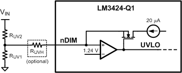
The nDIM pin is a dual-function input that features an accurate 1.24V threshold with programmable hysteresis as shown in Figure 30. This pin functions as both the PWM dimming input for the LEDs and as a VIN UVLO. When the pin voltage rises and exceeds the 1.24V threshold, 20 µA (typical) of current is driven out of the nDIM pin into the resistor divider providing programmable hysteresis.
 Figure 30. UVLO Circuit
 When using the nDIM pin for UVLO and PWM dimming concurrently, the UVLO circuit can have an extra series resistor to set the hysteresis. This allows the standard resistor divider to have smaller resistor values minimizing PWM delays due to a pull-down MOSFET at the nDIM pin (see PWM Dimming section). In general, at least 3V of hysteresis is preferable when PWM dimming, if operating near the UVLO threshold.
The turn-on threshold (VTURN-ON) is defined as follows:

The hysteresis (VHYS) is defined as follows: